Microchip PIC32MX120F032D Handleiding


Lees hieronder de 📖 handleiding in het Nederlandse voor Microchip PIC32MX120F032D (84 pagina's) in de categorie Niet gecategoriseerd. Deze handleiding was nuttig voor 44 personen en werd door 2 gebruikers gemiddeld met 4.5 sterren beoordeeld

Pagina 1/84
2007-2021 Microchip Technology Inc. DS60001145AA-page 1
PIC32
1.0 DEVICE OVERVIEW
This document defines the Flash programming
specification for the PIC32 family of 32-bit
microcontrollers.
This programming specification is designed to guide
developers of external programmer tools. Customers
who are developing applications for PIC32 devices
should use development tools that already provide
support for device programming.
The major topics of discussion include:
Section 1.0 “Device Overview”
Section 2.0 “Programming Overview”
Section 3.0 “Programming Steps”
Section 4.0 “Connecting to the Device
Section 5.0 “EJTAG vs. ICSP
Section 6.0 “Pseudo Operations”
Section 7.0 “Entering 2-Wire Enhanced ICSP
Mode”
Section 8.0 “Check Device Status”
Section 9.0 “Erasing the Device
Section 10.0 “Entering Serial Execution Mode”
Section 11.0 “Downloading the Programming
Executive (PE)”
Section 12.0 “Downloading a Data Block”
Section 13.0 “Initiating a Page Erase”
Section 14.0 “Initiating a Flash Row Write”
Section “”
Section 16.0 “Exiting Programming Mode”
Section 17.0 “The Programming Executive”
Section 18.0 “Checksum”
Section 19.0 “Configuration Memory and Device
ID”
Section 20.0 “TAP Controllers”
Section 21.0 “AC/DC Characteristics and Timing
Requirements”
Appendix A: “PIC32 Flash Memory Map”
Appendix B: “Hex File Format”
Appendix C: “Device IDs”
Appendix D: “Revision History”
2.0 PROGRAMMING OVERVIEW
When in development of a programming tool, it is
necessary to understand the internal Flash program
operations of the target device and the Special
Function Registers (SFRs) used to control Flash
programming, as these same operations and registers
are used by an external programming tool and its
software. These operations and control registers are
described in the “Flash Program Memory” chapter in
the specific device data sheet, and the related “PIC32
Family Reference Manual” section. It is highly
recommended that these documents be used in
conjunction with this programming specification.
An external tool programming setup consists of an
external programmer tool and a target PIC32 device.
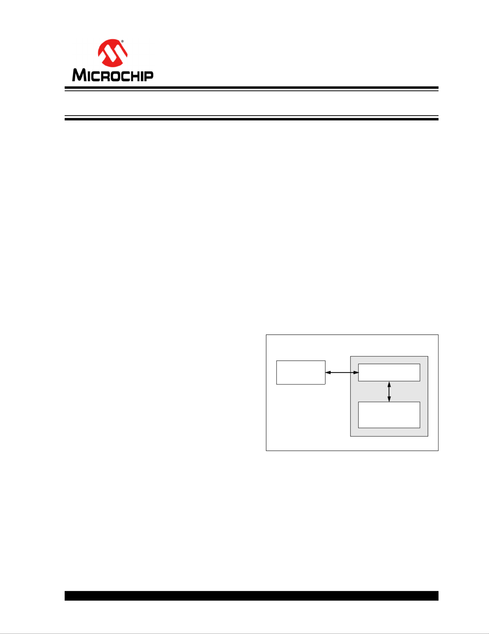
Figure 2-1 illustrates a typical programming setup. The
programmer tool is responsible for executing
necessary programming steps and completing the
programming operation.
FIGURE 2-1: PROGRAMMING SYSTEM
SETUP
Target PIC32 Device
CPU
On-Chip Memory
External
Programmer
PIC32 Flash Programming Specification
PIC32
DS60001145AA-page 2 2007-2021 Microchip Technology Inc.
2.1 Devices with Dual Flash Panel and
Dual Boot Regions
The PIC32MKXXXXXXD/E/F/K/L/M and PIC32MZ
families of devices incorporate several features useful
for field (self) programming of the device. These
features include dual Flash panels with dual boot
regions, an aliasing scheme for the boot regions
allowing automatic selection of boot code at start-up
and a panel swap feature for Program Flash. The two
Flash panels and their associated boot regions can be
erased and programmed separately. Refer to the
Section 48. “Memory Organization and
Permissions” (DS60001214) of the “PIC32 Family
Reference Manual” for a detailed explanation of these
features.
A development tool used for production programming
will not be concerned about most of these features with
the following exceptions:
Ensuring the SWAP bit (NVMCON[7]) is in the
proper setting. The default setting is ‘0 for no swap
of panels. The development tool should assume the
default setting when generating source files for the
programming tool.
Proper handling of the aliasing of the boot memory
in the checksum calculation. The aliased sections
will be duplicates of the fixed sections. See
Section 18.0 “Checksum” for more information on
checksum calculations with aliased regions
For PIC32MK devices, using the Erase/Retry
feature when an attempt to erase a Flash page fails
and needs to be retried. See Section 13.0
“Initiating a Page Erase” for more information.
2.2 Programming Interfaces
All PIC32 devices provide two physical interfaces to the
external programmer tool:
2-wire In-Circuit Serial Programming™ (ICSP™)
4-wire Joint Test Action Group (JTAG)
See Section 4.0 “Connecting to the Device” for
more information.
Either of these methods may use a downloadable
Programming Executive (PE). The PE executes from
the target device RAM and hides device programming
details from the programmer. It also removes overhead
associated with data transfer and improves overall data
throughput. Microchip has developed a PE that is
available for use with any external programmer, see
Section 17.0 “The Programming Executive” for
more information.
Section 3.0 “Programming Steps” describes high-
level programming steps, followed by a brief
explanation of each step. Detailed explanations are
available in corresponding sections of this document.
More information on programming commands, EJTAG,
and DC specifications are available in the following
sections:
Section 19.0 “Configuration Memory and
Device ID”
Section 20.0 “TAP Controllers”
Section 21.0 “AC/DC Characteristics and
Timing Requirements”
2.3 Enhanced JTAG (EJTAG)
The 2-wire and 4-wire interfaces use the EJTAG
protocol to exchange data with the programmer. While
this document provides a working description of this
protocol as needed, advanced users are advised to
refer to the Imagination Technologies Limited web site
(www.imgtec.com) for more information.
2.4 Data Sizes
Data sizes are defined as follows:
One word: 32 bits
One-half word: 16 bits
One-quarter word: 8 bits
One Byte: 8 bits
2007-2021 Microchip Technology Inc. DS60001145AA-page 3
PIC32
3.0 PROGRAMMING STEPS
All tool programmers must perform a common set of
steps, regardless of the actual method being used.
Figure 3-1 shows the set of steps to program PIC32
devices.
FIGURE 3-1: PROGRAMMING FLOW
The following sequence lists the programming steps
with a brief explanation of each step. More detailed
information about these steps is available in the
subsequent sections.
1. Connect to the target device.
To ensure successful programming, all required
pins must be connected to appropriate signals.
See Section 4.0 “Connecting to the Device”
for more information.
2. Place the target device in programming mode.
For 2-wire programming methods, the target
device must be placed in a special programming
mode (Enhanced ICSP™) before executing any
other steps.
See Section 7.0 “Entering 2-Wire Enhanced
ICSP Mode” for more information.
3. Check the status of the device.
Checks the status of the device to ensure it is
ready to receive information from the
programmer.
See Section 8.0 “Check Device Status” for
more information.
4. Erase the target device.
If the target memory block in the device is not
blank, or if the device is code-protected, an
erase step must be performed before
programming any new data.
See Section 9.0 “Erasing the Device” for
more information.
5. Enter programming mode.
Verifies that the device is not code-protected
and boots the TAP controller to start sending
and receiving data to and from the PIC32 CPU.
See Section 10.0 “Entering Serial Execution
Mode” for more information.
Done
Exit Programming Mode
Verify Device
Done
Initiate Flash Write
Download a Data Block
Download the PE
(Optional)
Enter Serial Exec Mode
Erase Device
Check Device Status
Start
Enter Enhanced ICSP™
(Only required for 2-wire)
No
Yes
Note: For the 4-wire programming methods,
Step 2 is not applicable.
PIC32
DS60001145AA-page 4 2007-2021 Microchip Technology Inc.
6. Download the Programming Executive (PE).
The PE is a small block of executable code that
is downloaded into the RAM of the target device.
It will receive and program the actual data.
See Section 11.0 “Downloading the
Programming Executive (PE)” for more
information.
7. Download the block of data to program.
All methods, with or without the PE, must
download the desired programming data into a
block of memory in RAM.
See Section 12.0 “Downloading a Data
Block” for more information.
8. Initiate Flash Write.
After downloading each block of data into RAM,
the programming sequence must be started to
program it into the target device’s Flash
memory.
See Section 14.0 “Initiating a Flash Row
Write for more information.
9. Repeat Step 7 and Step 8 until all data blocks
are downloaded and programmed.
10. Verify the program memory.
After all programming data and Configuration
bits are programmed, the target device memory
should be read back and verified for the
matching content.
See Section “” for more information.
11. Exit the programming mode.
The newly programmed data is not effective until
either power is removed and reapplied to the
target device or an exit programming sequence
is performed.
See Section 16.0 “Exiting Programming
Mode” for more information.
Note: If the programming method being used
does not require the PE, Step 6 is not
applicable.
2007-2021 Microchip Technology Inc. DS60001145AA-page 5
PIC32
4.0 CONNECTING TO THE DEVICE
The PIC32 family provides two possible physical
interfaces for connecting and programming the
memory contents, see Figure 4-1. For all programming
interfaces, the target device must be powered and all
required signals must be connected. In addition, the
interface must be enabled, either through its
Configuration bit, as in the case of the JTAG 4-wire
interface, or though a special initialization sequence, as
is the case for the 2-wire ICSP interface.
The JTAG interface is enabled by default in blank
devices shipped from the factory.
Enabling ICSP is described in Section 7.0 “Entering
2-Wire Enhanced ICSP Mode”.
FIGURE 4-1: PROGRAMMING
INTERFACES
4.1 4-wire Interface
One possible interface is the 4-wire JTAG (IEEE
1149.1) port. Table 4-1 lists the required pin
connections. This interface uses the following four
communication lines to transfer data to and from the
PIC32 device being programmed:
Test Clock Input (TCK)
Test Mode Select Input (TMS)
Test Data Input (TDI)
Test Data Output (TDO)
Refer to the specific device data sheet for the
connection of the signals to the device pins.
4.1.1 TEST CLOCK INPUT (TCK)
TCK is the clock that controls the updating of the TAP
controller and the shifting of data through the Instruc-
tion or selected Data registers. TCK is independent of
the processor clock with respect to both frequency and
phase.
4.1.2 TEST MODE SELECT INPUT (TMS)
TMS is the control signal for the TAP controller. This
signal is sampled on the rising edge of TCK.
4.1.3 TEST DATA INPUT (TDI)
TDI is the test data input to the Instruction or selected
Data register. This signal is sampled on the rising edge
of TCK for some TAP controller states.
4.1.4 TEST DATA OUTPUT (TDO)
TDO is the test data output from the Instruction or Data
registers. This signal changes on the falling edge of
TCK. TDO is only driven when data is shifted out,
otherwise the TDO is tri-stated.
TABLE 4-1: 4-WIRE INTERFACE PINS
Programmer
2-wire
ICSP™
OR
4-wire
JTAG
+
MCLR, V
DD
CORE
(1)
, V
DDR
1
V
8
(1)
,
PIC32
V
DD
IO
, V
SS
, V
SS
1
V
8
(1)
Note 1: This pin is not available on all devices.
Refer to the Pin Diagrams” or “Pin
Tables” section in the specific device data
sheet to determine availability.
Device Pin Name Pin
Type Pin Description
MCLR I Programming Enable
ENVREG(2) I Enable for On-Chip Voltage Regulator
VDD, VDDIO, VDDCORE
(2), VDDR1 8V(2), VBAT(2),
and AVDD(1) P Power Supply
VSS SS, V 1 8V(2)
, and AVSS(1) P Ground
VCAP(2) P CPU logic filter capacitor connection
TDI I Test Data In
TDO O Test Data Out
TCK I Test Clock
TMS I Test Mode State
Legend: I = Input O = Output P = Power
Note 1: All power supply and ground pins must be connected, including analog supplies (AV
DD) and ground (AVSS).
2: This pin is not available on all devices. Refer to the “Pin Diagrams” or “Pin Tables” section in the specific
device data sheet to determine availability.
PIC32
DS60001145AA-page 6 2007-2021 Microchip Technology Inc.
4.2 2-wire Interface
Another possible interface is the 2-wire ICSP port.
Table 4-2 lists the required pin connections. This
interface uses the following two communication lines to
transfer data to and from the PIC32 device being
programmed:
Serial Program Clock (PGECx)
Serial Program Data (PGEDx)
These signals are described in the following two
sections. Refer to the specific device data sheet for the
connection of the signals to the chip pins.
4.2.1 SERIAL PROGRAM CLOCK
(PGECX)
PGECx is the clock that controls the updating of the
TAP controller and the shifting of data through the
Instruction or selected Data registers. PGECx is
independent of the processor clock, with respect to
both frequency and phase.
4.2.2 SERIAL PROGRAM DATA (PGEDX)
PGEDx is the data input/output to the Instruction or
selected Data Registers, it is also the control signal for
the TAP controller. This signal is sampled on the falling
edge of PGECx for some TAP controller states.
TABLE 4-2: 2-WIRE INTERFACE PINS
Device
Pin Name
Programmer
Pin Name Pin Type Pin Description
MCLR MCLR P Programming Enable
ENVREG(2) N/A I Enable for On-Chip Voltage Regulator
VDD, VDDIO, VBAT(2), and AVDD(1) VDD P Power Supply
VDDCORE(2) and VDDR1 8V(2) N/A P Power Supply for DDR Interface
VSS, VSS1 8V(2), and AVSS
(1) VSS P Ground
VCAP(2) N/A P CPU Logic Filter Capacitor Connection
PGECx PGEC I Primary Programming Pin Pair: Serial Clock
PGEDx PGED I/O Primary Programming Pin Pair: Serial Data
Legend: I = Input O = Output P = Power
Note 1: All power supply and ground pins must be connected, including analog supplies (AV
DD) and ground (AVSS).
2: This pin is not available on all devices. Refer to either the “Pin Diagrams” or “Pin Tables” section in the
specific device data sheet to determine availability.
2007-2021 Microchip Technology Inc. DS60001145AA-page 7
PIC32
4.3 PIC32MX Power Requirements
Devices in the PIC32MX family are dual voltage
supply designs. There is one supply for the core and
another for peripherals and I/O pins. All devices
contain an on-chip regulator for the lower voltage
core supply to eliminate the need for an additional
external regulator. There are three implementations
of the on board regulator:
The first version has an internal regulator that can
be disabled using the ENVREG pin. When disabled,
an external power supply must be used to power the
core. If enabled, a low-ESR filter capacitor must be
connected to the VCAP pin, see Figure 4-2.
The second version has an internal regulator that
cannot be disabled. A low-ESR filter capacitor must
always be connected to the VCAP pin.
The third version has an internal regulator that
cannot be disabled and does not require a filter
capacitor
Refer to Section 21.0 “AC/DC Characteristics and
Timing Requirements” and the “Electrical
Characteristics” chapter in the specific device data
sheet for the power requirements for your device.
FIGURE 4-2: INTERNAL REGULATOR
ENABLE/DISABLE
OPTIONS
4.4 PIC32MX With VBAT Pin Power
Requirements
Some devices in the PIC32MX family provide a VBAT
pin which can be connected to the VDD power supply
during programming. See Figure 4-3.
FIGURE 4-3: PIC32MX WITH VBAT PIN
POWER CONNECTIONS
4.5 PIC32MZ EC and PIC32MZ EF
Power Requirements
Devices in the PIC32MZ EC and PIC32MZ EF families
are also dual voltage supply designs like PIC32MX
devices. However, the internal regulator does not
require the external filter capacitor, and there is no cor-
responding VCAP or ENVREG pins. See Figure 4-4.
Refer to Section 21.0 “AC/DC Characteristics and
Timing Requirements” and the “Electrical
Characteristics” chapter in the specific device data
sheet for the power requirements for your device.
FIGURE 4-4: PIC32MZ EC/EF POWER
CONNECTIONS
VDD
ENVREG
VCAP
VSS
PIC32MX
3.3V(1)
1.8V(1)
VDD
ENVREG
VCAP
VSS
PIC32MX
CEFC
3.3V
Regulator Enabled(2)
Regulator Disabled(2)
(10 F typical)
Note 1: These are typical operating voltages. Refer to
Section 21.0 “AC/DC Characteristics and Timing
Requirements
for the full operating ranges of VDD
and VCAP.
2: Regulator Enabled and Regulator Disabled mode
are not available on all devices. Refer to the specific
device data sheet to determine availability.
(ENVREG tied to VDD)
(ENVREG tied to ground)
Note 1: This is typical operating voltage. Refer to
Section 21.0 “AC/DC Characteristics and Timing
Requirements
for the full operating range of VDD.
VDD
VBAT
VCAP
VSS
PIC32MX XLP
3.3V (1)
VDD
VSS
PIC32MZ EC/EF
3.3V(1)
Note 1: This is typical operating voltage. Refer to
Section 21.0 “AC/DC Characteristics and Timing
Requirements
for the full operating range of VDD.
PIC32
DS60001145AA-page 8 2007-2021 Microchip Technology Inc.
4.6 PIC32MZ DA Power Requirements
Devices in the PIC32MZ DA family are quadruple
voltage supply designs. Two of the voltage supplies are
identical to the PIC32MZ EC and PIC32MZ EF voltage
supplies. The third voltage supply is for the DDR
memory interface, and requires a 1.8 volt supply. The
fourth voltage supply is for the VBAT pin, but it can be
connected to the VDD power supply. See Figure 4-5.
Refer to Section 21.0 “AC/DC Characteristics and
Timing Requirements” and the “Electrical
Characteristics” chapter in the specific device data
sheet for the power requirements for your device.
FIGURE 4-5: PIC32MZ DA POWER
CONNECTIONS
4.7 PIC32MK Power Requirements
Devices in the PIC32MK family are triple voltage supply
designs. Two of the voltage supplies are identical to the
PIC32MZ EC and PIC32MZ EF voltage supplies. The
third voltage supply is for the VBAT pin, but it can be
connected to the VDD power supply. See Figure 4-6.
FIGURE 4-6: PIC32MK POWER
CONNECTIONS
4.8 PIC32MZ W1 Power Requirements
Devices in the PIC32MZ W1 family are triple voltage
supply designs. Two of the voltage supplies are identi-
cal to the PIC32MZ EC and PIC32MZ EF voltage sup-
plies. Connect the voltage supplies of the PIC32MZ W1
family of devices as shown in the following figure.
FIGURE 4-7: PIC32MZ W1 POWER
CONNECTIONS
VDDIO
VBAT
VDDCORE and VDDR1V8
VSS
PIC32MZ DA
3.3V(1)
1.8V(1)
Note 1: These are typical operating voltages. Refer to
Section 21.0 “AC/DC Characteristics and Timing
Requirements
for the full operating ranges of
VDDIO, VBAT, VDDCORE and VDDR1 8V.
VSS1 8V
VDD
VBAT
VSS
PIC32MK
3.3V(1)
Note 1: These are typical operating voltages. Refer to
Section 21.0 “AC/DC Characteristics and Timing
Requirements
for the full operating ranges of VDD
and VBAT.
VDD
VBAT
VSS
PIC32MZ W1
3.3V(1)
Note 1: These are typical operating voltages. Refer to
Section 21.0 “AC/DC Characteristics and Timing
Requirements
for the full operating ranges of VDD
and VBAT.
2007-2021 Microchip Technology Inc. DS60001145AA-page 9
PIC32
5.0 EJTAG vs. ICSP
Programming is accomplished through the EJTAG
module in the CPU core. EJTAG is connected to either
the full set of JTAG pins or a reduced 2-wire to 4-wire
EJTAG interface for ICSP mode. In both modes,
programming of the PIC32 Flash memory is
accomplished through the ETAP controller. The TAP
Controller uses the TMS pin to determine if Instruction
or Data registers should be accessed in the shift path
between TDI and TDO, see Figure 5-1.
The basic concept of EJTAG that is used for
programming is the use of a special memory area
called DMSEG (0xFF200000 to 0xFF2FFFFF), which
is only available when the processor is running in
Debug mode. All instructions are serially shifted into an
internal buffer, and then loaded into the Instruction
register and executed by the CPU. Instructions are fed
through the ETAP state machine in 32-bit groups.
FIGURE 5-1: TAP CONTROLLER
5.1 Programming Interface
Figure 5-2 shows the basic programming interface in
PIC32 devices. Descriptions of each interface block are
provided in subsequent sections.
FIGURE 5-2: BASIC PIC32 PROGRAMMING INTERFACE BLOCK DIAGRAM
5.1.1 ETAP
This block serially feeds instructions and data into the
CPU.
5.1.2 MTAP
In addition to the EJTAG TAP (ETAP) controller, the
PIC32 device uses a second proprietary TAP controller
for additional operations. The Microchip TAP (MTAP)
controller supports two instructions relevant to
programming: MTAP_COMMAND and TAP switch
Instructions. See Table 20-1 for a complete list of
Instructions. The MTAP_COMMAND instruction provides
a mechanism for a JTAG probe to send commands to
the device through its Data register.
The programmer sends commands by shifting in the
MTAP_COMMAND SendCommand instruction through the
pseudo operation, and then sending the MTAP_COM-
MAND DR commands through the XferData pseudo
operation, see Table 20-2 for specific commands.
The probe does not need to issue a MTAP_COMMAND
instruction for every command shifted into the Data
register.
TMS
TCK
TDO
TDI
Tap Controller
Instruction, Data,
and Control Registers
TMS
TCK
TDI
TDO
or
PGECx
PGEDx
ETAP CPU
MTAP
2-wire
Flash
Flash
to
4-wire
Controller
Memory
Common
VDD DD DD/V IO/V 1 8VCORE
VSS/VSS
1
V
8
MCLR
VBAT/VDDR
1
V
8
PIC32
DS60001145AA-page 10 2007-2021 Microchip Technology Inc.
5.1.3 2-WIRE TO 4-WIRE
This block converts the 2-wire ICSP interface to the
4-wire JTAG interface.
5.1.4 CPU
The CPU executes instructions at 8 MHz through the
internal oscillator.
5.1.5 FLASH CONTROLLER
The Flash controller controls erasing and programming
of the Flash memory on the device.
5.1.6 FLASH MEMORY
The PIC32 device Flash memory is divided into two
logical Flash partitions consisting of the Boot Flash
Memory (BFM) and Program Flash Memory (PFM).
The BFM begins at address 0x1FC00000, and the PFM
begins at address 0x1D000000. Each Flash partition is
divided into pages, which represent the smallest block
of memory that can be erased. Depending on the
device, page sizes are 256 words (1024 bytes), 1024
words (4096 bytes) or 4096 words (16,384 bytes). Row
size indicates the number of words that are
programmed with the row program command. There
are always 8 rows within a page; therefore, devices
with 256, 1024, and 4096 word page sizes have 32,
128, and 512 word row sizes, respectively. Table 5-1
shows the PFM, BFM, row, and page size of each
device family.
For a PIC32MZ W1 device, the BFM begins at address
0x1FC00000, and the PFM begins at address
0x10000000. The Flash is divided into pages of 1024
words or 4 kbytes, which represents the smallest block
of memory that can be erased. Row size indicates the
number of words that are programmed with row
program commands. The Flash contains 4 rows within
a page with a total row size of 256 words or 1024 bytes.
Memory locations of the BFM are reserved for the
device Configuration registers, see Section 19.0
“Configuration Memory and Device ID for more
information.
TABLE 5-1: CODE MEMORY SIZE
PIC32 Device Row Size
(Words)
Page Size
(Words)
Boot Flash Memory Address
(Bytes) (See Note 1)
Programming Executive
(See Notes 2 and 3)
PIC32MX
110/120/130/150/170
210/220/230/350/270
(28/36/44-pin devices Only)
32 256
0x1FC00000-0x1FC00BFF (3 KB)
RIPE_11_aabbcc.hex
PIC32MX
120/130/150/170/230/250/
270/530/550/570
(64/100-pin devices Only)
PIC32MX
15X/17X/25X/27X
(28/44-pin devices Only)
0x1FC00000-0x1FC02FFF (12 KB)
PIC32MZ W1 256 1024 0x1FC00000-0x1FC0FFFF (64 KB)
Note 1: Program Flash Memory address ranges are based on Program Flash size are as given below:
0x1D000000-0x1D003FFF (16 KB)
0x1D000000-0x1D007FFF (32 KB)
0x1D000000-0x1D00FFFF (64 KB)
0x1D000000-0x1D01FFFF (128 KB)
0x1D000000-0x1D03FFFF (256 KB)
0x1D000000-0x1D07FFFF (512 KB)
0x1D000000-0x1D0FFFFF (1024 KB)
0x1D000000-0x1D1FFFFF (2048 KB)
All Program Flash memory sizes are not supported by each family.
Program Flash Memory address ranges for PIC32MZ W1: 0x10000000-0x100FFFFF (1024 KB).
2: The Programming Executive can be obtained from the related product page on the Microchip website or it can be
located in the following MPLAB ® X IDE installation folders:
…\Microchip\MPLABX\<version>\mplab_ide\mplablibs\modules\ext\REALICE.jar
…\Microchip\MPLABX\<version>\mplab_ide\mplablibs\modules\ext\ICD3.jar
…\Microchip\MPLABX\<version>\mplab_ide\mplablibs\modules\ext\PICKIT3.jar
3: The last characters of the file name, aabbcc, vary based on the revision of the file.
2007-2021 Microchip Technology Inc. DS60001145AA-page 11
PIC32
PIC32MX
330/350/370/430/450/470
128 1024 0x1FC00000-0x1FC02FFF (12 KB) RIPE_06_aabbcc.hex
PIC32MX
320/340/360/420/440/460
PIC32MX
534/564/664/764
PIC32MX
575/675/695/795
PIC32MK
0512/1024XXD/E/F/K/L/M 128 1024 0x1FC00000-0x1FC04FFF (20 KB)
0x1FC20000-0x1FC24FFF (20 KB) RIPE_15a_aabbcc.hex
PIC32MK
0256/0512XXG/H 128 1024 0x1FC00000-0x1FC04FFF (20 KB) RIPE_15a_aabbcc.hex
PIC32MZ
05XX/10XX/20XX 512 4096 0x1FC00000-0x1FC13FFF (80 KB)
0x1FC20000-0x1FC33FFF (80 KB) RIPE_15_aabbcc.hex
PIC32MZ W1 256 1024 0x1FC00000-0x1FC0FFFF (64 KB) RIPE_25_aabbcc.hex
TABLE 5-1: CODE MEMORY SIZE (CONTINUED)
PIC32 Device Row Size
(Words)
Page Size
(Words)
Boot Flash Memory Address
(Bytes) (See Note 1)
Programming Executive
(See Notes 2 and 3)
Note 1: Program Flash Memory address ranges are based on Program Flash size are as given below:
0x1D000000-0x1D003FFF (16 KB)
0x1D000000-0x1D007FFF (32 KB)
0x1D000000-0x1D00FFFF (64 KB)
0x1D000000-0x1D01FFFF (128 KB)
0x1D000000-0x1D03FFFF (256 KB)
0x1D000000-0x1D07FFFF (512 KB)
0x1D000000-0x1D0FFFFF (1024 KB)
0x1D000000-0x1D1FFFFF (2048 KB)
All Program Flash memory sizes are not supported by each family.
Program Flash Memory address ranges for PIC32MZ W1: 0x10000000-0x100FFFFF (1024 KB).
2: The Programming Executive can be obtained from the related product page on the Microchip website or it can be
located in the following MPLAB ® X IDE installation folders:
…\Microchip\MPLABX\<version>\mplab_ide\mplablibs\modules\ext\REALICE.jar
…\Microchip\MPLABX\<version>\mplab_ide\mplablibs\modules\ext\ICD3.jar
…\Microchip\MPLABX\<version>\mplab_ide\mplablibs\modules\ext\PICKIT3.jar
3: The last characters of the file name, aabbcc, vary based on the revision of the file.
PIC32
DS60001145AA-page 12  2007-2021 Microchip Technology Inc.
5.2 4-wire JTAG Details
The 4-wire interface uses standard JTAG (IEEE
1149.1-2001) interface signals.
TCK: Test Clock – drives data in/out
TMS: Test Mode Select – selects operational mode
TDI: Test Data Input – data into the device
TDO: Test Data Output – data out of the device
Since only one data line is available, the protocol is
necessarily serial (like SPI). The clock input is at the
TCK pin. Configuration is performed by manipulating a
state machine bit by bit through the TMS pin. One bit of
data is transferred in and out per TCK clock pulse at the
TDI and TDO pins. Different instruction modes can be
loaded to read the chip ID or manipulate chip functions.
Data presented to TDI must be valid for a chip-specific
setup time before, and hold time, after the rising edge
of TCK. TDO data is valid for a chip-specific time after
the falling edge of TCK, refer to Figure 5-3.
FIGURE 5-3: 4-WIRE JTAG INTERFACE
TMS
TDI
TDO
iMSb
iLSb
‘ ’1
TCK
oLSb oMSb
‘ ’1 ‘ ’1 ‘ ’1
‘ ’0 ‘ ’0 ‘ ’0
 2007-2021 Microchip Technology Inc. DS60001145AA-page 13
PIC32
5.3 2-wire ICSP Details
In ICSP mode, the 2-wire ICSP signals are time
multiplexed into the 2-wire to 4-wire block. The 2-wire
to 4-wire block then converts the signals to look like a
4-wire JTAG port to the TAP controller. The following
are two possible modes of operation:
4-phase ICSP
2-phase ICSP
5.3.1 4-PHASE ICSP
In 4-phase ICSP mode, the TDI, TDO and TMS device
pins are multiplexed onto PGEDx in four clocks, see
Figure 5-4. The Least Significant bit (LSb) is shifted
first; and TDI and TMS are sampled on the falling edge
of PGECx, while TDO is driven on the falling edge of
PGECx. The 4-phase ICSP mode is used for both read
and write data transfers.
5.3.2 2-PHASE ICSP
In 2-phase ICSP mode, the TMS and TDI device pins
are multiplexed into PGEDx in two clocks, see
Figure 5-5. The LSb is shifted first; and TDI and TMS
are sampled on the falling edge of PGECx. There is no
TDO output provided in this mode. The 2-phase ICSP
mode was designed to accelerate 2-wire, write-only
transactions.
FIGURE 5-4: 2-WIRE, 4-PHASE
Note: The packet is not actually executed until
the first clock of the next packet. To enter
2-wire, 2-phase ICSP mode, the TDOEN
bit (DDPCON[0] or CFGCON[0]) must be
set to ‘0’.
TMS
TDI
TDO
IR4
IR0
‘ ’1
TCK
‘ ’1‘ ’1‘ ’1
‘ ’0‘ ’0‘ ’0
X
1
PGECx
PGEDx pTDO = 1
TDI = IR0
TMS = 0nTDO = 0
PIC32
DS60001145AA-page 14 2007-2021 Microchip Technology Inc.
FIGURE 5-5: 2-WIRE, 2-PHASE
5.3.3 SYNCHRONIZATION
Some PIC32 devices can Reset the internal EJTAG
state machine if the attached programmer loses syn-
chronization with it. This can occur when noise is pres-
ent on the PGCx signal.
To achieve resynchronization, the PGEDx pin is held
high for 24 PGECx clock cycles. This forces five TMS
events into the EJTAG controller and will place the
EJTAG state machine into a Test Idle Reset. See
Figure 5-6 for an example of how to achieve
resynchronization.
When asserting the PGEDx pin high, there may be
contention on the pin as the device may attempt to
drive TDO out onto the pin while the in-circuit emulator
is driving in. This will only occur for a maximum of one
cycle as TMS high will advance the EJTAG state
machine out of a Shift-IR or Shift-DR state.
Synchronization in 2-wire, 2-phase mode is not
supported.
FIGURE 5-6: ACHIEVING RESYNCHRONIZATION
TMS
TDI
TDO
IR4
IR0
‘ ’1
TCK
‘ ’1‘ ’1‘ ’1
‘ ’0‘ ’0‘ ’0
X
1
PGECx
PGEDx
TDI = IR0
TMS = 0
2007-2021 Microchip Technology Inc. DS60001145AA-page 15
PIC32
6.0 PSEUDO OPERATIONS
To simplify the description of programming details, all
operations will be described using pseudo operations.
There are several functions used in the pseudo-code
descriptions. These are used either to make the
pseudo-code more readable, to abstract
implementation-specific behavior or both. When
passing parameters with pseudo operation, the
following syntax will be used:
5’h0x03 – send 5-bit hexadecimal value of 3
6’b011111 – send 6-bit binary value of 31
These functions are defined in this section, and include
the following operations:
SetMode (mode)
SendCommand (command)
oData = XferData (iData)
oData = XferFastData (iData)
oData = XferInstruction (instruction)
6.1 SetMode Pseudo Operation
Format:
SetMode (mode)
Purpose:
To set the EJTAG state machine to a specific state.
Description:
The value of mode is clocked into the device on
signal TMS. TDI is set to a ‘0 and TDO is ignored.
Restrictions:
None.
Example:
SetMode (6’b011111)
FIGURE 6-1: SetMode 4-WIRE
FIGURE 6-2: SetMode 2-WIRE
TMS
TDI
TDO
‘ ’1
TCK
‘ ’1‘ ’1‘ ’1‘ ’1‘ ’0
Mode = 6’b011111
PGEDx
PGECx
TDI = 0TDO = 1
TMS = 1TDI = 0TMS = 0TDO = x
Mode = 6’b011111
PIC32
DS60001145AA-page 16 2007-2021 Microchip Technology Inc.
6.2 SendCommand Pseudo Operation
Format:
SendCommand (command)
Purpose:
To send a command to select a specific TAP register.
Description (in sequence):
1. The TMS Header is clocked into the device to
select the Shift IR state
2. The command is clocked into the device on
TDI while holding signal TMS low.
3. The last Most Significant bit (MSb) of the
command is clocked in while setting TMS
high.
4. The TMS Footer is clocked in on TMS to return
the TAP controller to the Run/Test Idle state.
Restrictions:
None.
Example:
SendCommand (5’h0x07)
FIGURE 6-3: SendCommand 4-WIRE
FIGURE 6-4: SendCommand 2-WIRE (4-PHASE)
TMS
TDI
TDO
iMSb
‘ ’1
TCK
‘ ’ 1 1’ ‘10’ ‘0 0 ‘ ’
x
1
iLSb
TMS Header = 1100 Command = 5’h0x07 Command (MSb)
+ TMS = 1TMS Footer = 10
TDI =
0
TMS =
1
TMS =
1
TDI =
0
TDO =
x
TDO =
x
TDI = iMSb
TDO =
x
TMS =
0
TDI = iLSb
TDO =
x
TMS =
1
TMS Header = 1100 Command (5’h0x07) + TMS = 0Command (MSb) + TMS = 1TMS Footer = 10
PGECx
PGEDx
2007-2021 Microchip Technology Inc. DS60001145AA-page 17
PIC32
6.3 XferData Pseudo Operation
Format:
oData = XferData (iData)
Purpose:
To clock data to and from the register selected by the
command.
Description (in sequence):
1. The TMS Header is clocked into the device to
select the Shift DR state.
2. The data is clocked in/out of the device on
TDI/TDO while holding signal TMS low.
3. The last MSb of the data is clocked in/out
while setting TMS high.
4. The TMS Footer is clocked in on TMS to return
the TAP controller to the Run/Test Idle state.
Restrictions:
None.
Example:
oData = XferData (32’h0x12)
FIGURE 6-5: XferData 4-WIRE
FIGURE 6-6: XferData 2-WIRE (4-PHASE)
TMS
TDI
TDO
iMSb
‘ ’1
TCK
‘ ’1‘ ’1
‘ ’0‘ ’0‘ ’0
iLSb
TMS Header = 100 Data (32’h0x12) Data (MSb) + TMS = 1TMS Footer = 10
oMSboLSb
TDI = 0TMS = 0
TDO = oLSb
TDI = 0TDO = XTMS = 0TDI = 0TDO = XTMS = 1
PGEC
PGED
TMS Header = 100
TDI = 0TMS = 0TDO = XTDI = 0TDO = XTMS = 1
TMS = 1TDO = XTMS = 0TDI = iLSb
TDO = oLSb+1
TDI = iMSb
Data (31’h0x12) + TMS = 0Data (MSb) + TMS Footer = 1
TMS Footer = 10
...
PIC32
DS60001145AA-page 18 2007-2021 Microchip Technology Inc.
6.4 XferFastData Pseudo Operation
Format:
oData = XferFastData (iData)
Purpose:
To quickly send 32 bits of data in/out of the device.
Description (in sequence):
1. The TMS Header is clocked into the device to
select the Shift DR state.
2. The input value of the PrAcc bit, which is 0’, is
clocked in.
3. TMS Footer = 10 is clocked in to return the TAP
controller to the Run/Test Idle state.
Restrictions:
The SendCommand (ETAP_FASTDATA) must be sent
first to select the Fastdata register, as shown in
Example 6-1. See Table 20-4 for a detailed descriptions
of commands.
EXAMPLE 6-1: SendCommand
FIGURE 6-7: XferFastData 4-WIRE
FIGURE 6-8: XferFastData 2-WIRE (2-phase)
Note: For 2-wire (4-phase) on the last clock,
the oPrAcc bit is shifted out on TDO while
clocking in the TMS Header. If the value of
oPrAcc is not 1’, the whole operation
must be repeated.
Note: For 2-wire (4-phase) the TDO during this
operation will be the LSb of output data.
The rest of the 31 bits of the input data are
clocked in and the 31 bits of output data
are clocked out. For the last bit of the input
data, the TMS Footer = 1 is set.
Note: The 2-phase XferData is only used when
talking to the PE. See Section 17.0 “The
Programming Executive” for more
information.
// Select the Fastdata Register
SendCommand(ETAP_FASTDATA)
// Send/Receive 32-bit Data
oData = XferFastData(32’h0x12)
TMS
TDI
TDO
iMSb
iLSb
‘ ’1
TCK
oLSb oMSb
‘ ’1‘ ’1
‘ ’0‘ ’0‘ ’0
‘ ’0
‘ ’1
TMS Header = 100 PrAcc Data (32’h0x12) Data (MSb) + TMS = 1TMS Footer = 10
TDI = XTMS = 1
TDI = X
TDI =
TMS = 0
TDI =
TMS = 0TDI = 0TMS = 1
TMS Header = 100 Data (32’h0x12) TMS Footer = 10
iLSb
PGEDx
PGECx
PrAcc
TMS = 1
MSb
Data (MSb) TMS = 1
2007-2021 Microchip Technology Inc. DS60001145AA-page 19
PIC32
FIGURE 6-9: XferFastData 2-WIRE (4-PHASE)
TDI = 0TMS = 0TDO = oPrAccTDI = 0TDO = XTMS = 0TDI = 0TDO = XTMS = 1
PGECx
PGEDx
TMS Header = 100
TDI = 0TMS = 0TDO = XTDI = 0TDO = XTMS = 1
TMS = 1
TDO =
XTMS = 0TDI = iLSb TDO = oLSb+1 TDI = iMSb
Data (31’h12) + TMS = 0Data (MSb) + TMS Footer = 1
TMS Footer = 10
TMS = 0TDI = 0 TDO = oLSb
PrAcc
PIC32
DS60001145AA-page 20 2007-2021 Microchip Technology Inc.
6.5 XferInstruction Pseudo
Operation
Format:
XferInstruction (instruction)
Purpose:
To send 32 bits of data for the device to execute.
Description:
The instruction is clocked into the device and then
executed by CPU.
Restrictions:
The device must be in Debug mode.
EXAMPLE 6-2: XferInstruction
XferInstruction (instruction)
{
// Select Control Register
SendCommand(ETAP_CONTROL);
// Wait until CPU is ready
// Check if Processor Access bit (bit 18) is set
do {
controlVal = XferData(32’h0x0004C000);
} while( PrAcc(contorlVal[18]) is not ‘1’ );
// Select Data Register
SendCommand(ETAP_DATA);
// Send the instruction
XferData( );instruction
// Tell CPU to execute instruction
SendCommand(ETAP_CONTROL);
XferData(32’h0x0000C000);
}
2007-2021 Microchip Technology Inc. DS60001145AA-page 21
PIC32
6.6 ReadFromAddress Pseudo
Operation
Format:
oData = ReadFromAddress (address)
Purpose:
To send 32 bits of data to the device memory.
Description:
The 32-bit data is read from the memory at the
address specified in the “address” parameter.
Restrictions:
The device must be in Debug mode.
EXAMPLE 6-3: ReadFromAddress FOR PIC32MX, PIC32MZ AND PIC32MK DEVICES
ReadFromAddress (address)
{
// Load Fast Data register address to s3
instruction = 0x3c130000;
instruction |= (0xff200000>>16)&0x0000ffff;
XferInstruction(instruction); // lui s3, <FAST_DATA_REG_ADDRESS(31:16)> - set address of fast
data register
// Load memory address to be read into t0
instruction = 0x3c080000;
instruction |= (address>>16)&0x0000ffff;
XferInstruction(instruction); // lui t0, <DATA_ADDRESS(31:16)> - set address of data
instruction = 0x35080000;
instruction |= (address&0x0000ffff);
XferInstruction(instruction); // ori t0, <DATA_ADDRESS(15:0)> - set address of data
// Read data
XferInstruction(0x8d090000); // lw t1, 0(t0)
// Store data into Fast Data register
XferInstruction(0xae690000); // sw t1, 0(s3) - store data to fast data register
XferInstruction(0); // nop
// Shift out the data
SendCommand(ETAP_FASTDATA);
oData = XferFastData(32'h0x00000000);
return oData;
}
PIC32
DS60001145AA-page 22 2007-2021 Microchip Technology Inc.
6.7 Synchronize Pseudo Operation
Format:
Synchronize ()
Purpose:
To reset the EJTAG state machine into Test Idle
Reset.
Description:
The PGEDx signal is held high for 24 PGECx clock
cycles. All other signals are ignored.
Restrictions:
None.
FIGURE 6-10: ACHIEVING RESYNCHRONIZATION
2007-2021 Microchip Technology Inc. DS60001145AA-page 23
PIC32
7.0 ENTERING 2-WIRE ENHANCED
ICSP MODE
To use the 2-wire PGEDx and PGECx pins for pro-
gramming, they must be enabled. Note that any pair of
programming pins available on a particular device may
be used, however, they must be used as a pair. PGED1
must be used with PGEC1, and so on.
The following steps are required to enter 2-wire
Enhanced ICSP mode:
1. The MCLR pin is briefly driven high, then low.
2. A 32-bit key sequence is clocked into PGEDx.
3. The MCLR pin is then driven high within a
specified period of time and held.
Refer to Section 21.0 “AC/DC Characteristics and
Timing Requirements” for timing requirements.
The programming voltage applied to the MCLR pin is
VIH, which is essentially VDD, in PIC32 devices. There
is no minimum time requirement for holding at VIH.
After VIH is removed, an interval of at least P18 must
elapse before presenting the key sequence on PGEDx.
The key sequence is a specific 32-bit pattern: 0100
1101 0100 0011 0100 1000 0101 0000 (the
acronym ‘MCHP’, in ASCII). The device will enter
Program/Verify mode only if the key sequence is valid.
The MSb of the Most Significant nibble must be shifted
in first.
Once the key sequence is complete, VIH must be
applied to the MCLR pin and held at that level for as
long as the 2-wire Enhanced ICSP interface is to be
maintained. An interval of at least time P19 and P7
must elapse before presenting data on PGEDx. Signals
appearing on PGEDx before P7 has elapsed will not be
interpreted as valid.
Upon successful entry, the programming operations
documented in subsequent sections can be performed.
While in 2-wire Enhanced ICSP mode, all unused I/Os
are placed in the high-impedance state.
FIGURE 7-1: ENTERING ENHANCED ICSPMODE
Note: If using the 4-wire JTAG interface, the
following procedure is not necessary.
Note: Entry into ICSP mode places the device in
Reset to prevent instructions from
executing. To release the Reset, the
MCHP_DE_ASSERT_RST command must
be issued.
MCLR
PGEDx
PGECx
VDD
P6
P14
b31 b30 b29 b28 b27 b2 b1 b0b3
...
Program/Verify Entry Code = 0x4D434850
P1A
P1B
P18
P19
01001 0000
P7
VIH VIH
P20
PIC32
DS60001145AA-page 24 2007-2021 Microchip Technology Inc.
8.0 CHECK DEVICE STATUS
Before a device can be programmed, the programmer
must check the status of the device to ensure that it is
ready to receive information.
FIGURE 8-1: CHECK DEVICE STATUS
8.1 4-wire Interface
The setup sequence to enter 4-wire JTAG program-
ming should be done while asserting the MCLR pin.
Once the programming mode is entered, the MCLR pin
can be released to allow the processor to execute
instructions or drive ports.
The following steps are required to check the device
status using the 4-wire interface:
1. Set the MCLR pin low.
2. SetMode (6’b011111) to force the Chip TAP
controller into Run Test/Idle state.
3.
SendCommand
(MTAP_SW_MTAP).
4. SetMode (6’b011111) to force the Chip TAP
controller into Run Test/Idle state.
5. SendCommand (MTAP_COMMAND).
6. statusVal = XferData (MCHP_STATUS).
7. If CFGRDY (statusVal[3]) is not 1and FCBUSY
(statusVal[2]) is not ‘0 GOTO step 5.
8.2 2-wire Interface
The following steps are required to check the device
status using the 2-wire interface:
1. SetMode (6’b011111) to force the Chip TAP
controller into Run Test/Idle state.
2. SendCommand (MTAP_SW_MTAP).
3. SetMode (6’b011111) to force the Chip TAP
controller into Run Test/Idle state.
4. SendCommand (MTAP_COMMAND).
5. statusVal = XferData (MCHP_STATUS).
6. If CFGRDY (statusVal[3]) is not 1and FCBUSY
(statusVal[2]) is not ‘0’, GOTO step 4.
SetMode (6’b011111)
SendCommand MTAP_SW_MTAP ( )
SendCommand MTAP_COMMAND ( )
statusVal = XferData (MCHP_STATUS)
FCBUSY = 0
CFGRDY = 1
No
Set MCLR low 4-wire
Done
Yes
SetMode (6’b011111)
Note: If using the 4-wire interface, the oscillator
source, as selected by the Configuration
Words, must be present to access the
Flash memory. In an unprogrammed
device, the oscillator source is the internal
FRC allowing for Flash memory access. If
the Configuration Words have been
reprogrammed selecting an external
oscillator source then it must be present
for Flash memory access. See the
“Special Features” chapter in the
specific device data sheet for details
regarding oscillator selection using the
Configuration Word settings.
Note: If the CFGRDY and FCBUSY bits do not
come to the proper state within 10 ms, the
sequence may have been executed
incorrectly or the device is damaged.
2007-2021 Microchip Technology Inc. DS60001145AA-page 25
PIC32
9.0 ERASING THE DEVICE
Before a device can be programmed, it must be
erased. The erase operation writes all ‘1s’ to the Flash
memory and prepares it to program a new set of data.
Once a device is erased, it can be verified by
performing a “Blank Check” operation. See
Section 9.1 “Blank Check” for more information.
The procedure for erasing program memory (Program,
boot, and Configuration memory) consists of selecting
the MTAP and sending the MCHP_ERASE command.
The programmer must wait for the erase operation to
complete by reading and verifying bits in the
MCHP_STATUS value. Figure 9-1 illustrates the process
for performing a Chip Erase.
The following steps are required to erase a target
device:
1. SendCommand (MTAP_SW_MTAP).
2. SetMode (6’b011111).
3. SendCommand (MTAP_COMMAND).
4. XferData (MCHP_ERASE).
5. XferData (MCHP_DE_ASSERT_RST). This step is
not required for PIC32MX devices.
6. Delay 10 ms.
7. statusVal = XferData (MCHP_STATUS).
8. If CFGRDY (statusVal[3]) is not 1and FCBUSY
(statusVal[2]) is not 0’, GOTO to step 5.
FIGURE 9-1: ERASE DEVICE
9.1 Blank Check
The term “Blank Check” implies verifying that the
device has been successfully erased and has no
programmed memory locations. A blank or erased
memory location always reads as ‘1’.
The device Configuration registers are ignored by the
Blank Check. Additionally, all unimplemented memory
space should be ignored from the Blank Check.
Note: The Device ID memory locations are read-
only and cannot be erased. Therefore,
Chip Erase has no effect on these memory
locations.
Note: The Chip Erase operation is a self-timed
operation. If the FCBUSY and CFGRDY
bits do not set properly within the specified
Chip Erase time, the sequence may have
been executed incorrectly or the device is
damaged.
SendCommand (MTAP_COMMAND)
statusVal =
XferData (MCHP_STATUS)
FCBUSY
=
0
CFGRDY
=
1
No
SendCommand (MTAP_SW_MTAP)
Select MTAP
Put MTAP in Command Mode
XferData (MCHP_ERASE)
Issue Chip Erase Command
Read Erase Status
Done
Yes
10 milliseconds Delay
XferData (MCHP_DE_ASSERT_RST)
Not required for PIC32MX Devices
SetMode (6’b011111)
PIC32
DS60001145AA-page 26 2007-2021 Microchip Technology Inc.
10.0 ENTERING SERIAL
EXECUTION MODE
Before programming a device, it must be placed in
Serial Execution mode. The procedure for entering
Serial Execution mode consists of verifying that the
device is not code-protected. If the device is code-
protected, a Chip Erase must be performed. See
Section 9.0 “Erasing the Device for details.
FIGURE 10-1: ENTERING SERIAL
EXECUTION MODE
Select MTAP
SendCommand (MTAP_SW_MTAP)
Put MTAP in Command Mode
SendCommand (MTAP_COMMAND)
Read Code-Protect Status
statusVal = XferData (MCHP_STATUS)
CPS = 1Cannot Enter
Must Erase First
Select ETAP
SendCommand MTAP_SW_ETAP ( )
Put CPU in Serial Exec Mode
SendCommand (ETAP_EJTAGBOOT)
No
2-wire
4-wire
Set MCLR High
Enable Flash
XferData (MCHP_FLASH_EN)
Release Reset
XferData (MCHP_DE_ASSERT_RST)
Put MTAP in Command Mode
SendCommand MTAP_COMMAND ( )
Select MTAP
SendCommand MTAP_SW_MTAP ( )
Assert Reset
XferData (MCHP_ASSERT_RST)2-wire
Yes
Select ETAP
SendCommand MCHP_SW_ETAP ( )
Required for PIC32MX devices
SetMode (6’b011111)
SetMode (6’b011111)
SetMode (6’b011111)
SetMode (6’b011111)
2007-2021 Microchip Technology Inc. DS60001145AA-page 27
PIC32
10.1 4-wire Interface
The following steps are required to enter Serial
Execution mode:
1. SendCommand (MTAP_SW_MTAP).
2. SetMode (6’b011111).
3. SendCommand (MTAP_COMMAND).
4. statusVal = XferData (MCHP_STATUS).
5. If CPS (statusVal[7]) is not 1’, the device must
be erased first.
6. SendCommand (MTAP_SW_ETAP).
7. SetMode (6’b011111).
8. SendCommand (ETAP_EJTAGBOOT).
9. Set the MCLR pin high.
10.2 2-wire Interface
The following steps are required to enter Serial
Execution mode:
1. SendCommand (MTAP_SW_MTAP).
2. SetMode (6’b011111).
3. SendCommand (MTAP_COMMAND).
4. statusVal = XferData (MCHP_STATUS).
5. If CPS (statusVal[7]) is not 1’, the device must
be erased first.
6. XferData (MCHP_ASSERT_RST).
7. SendCommand (MTAP_SW_ETAP).
8. SetMode (6’b011111).
9. SendCommand (ETAP_EJTAGBOOT).
10. SendCommand (MTAP_SW_MTAP).
11. SetMode (6’b011111).
12. SendCommand (MTAP_COMMAND).
13. XferData (MCHP_DE_ASSERT_RST).
14. XferData (MCHP_FLASH_ENABLE). This step is
required for PIC32MX family devices.
15. SendCommand (MTAP_SW_ETAP).
16. SetMode (6’b011111).
Note: It is assumed that the MCLR pin has been
driven low from the previous Check
Device Status step (see Figure 8-1).
PIC32
DS60001145AA-page 28 2007-2021 Microchip Technology Inc.
11.0 DOWNLOADING THE
PROGRAMMING EXECUTIVE
(PE)
The PE resides in RAM memory and is executed by the
CPU to program the device. The PE provides the
mechanism for the programmer to program and verify
PIC32 devices using a simple command set and
communication protocol. There are several basic
functions provided by the PE:
Read memory
Erase memory
Program memory
Blank check
Read executive firmware revision
Get the Cyclic Redundancy Check (CRC) of Flash
memory locations
The PE performs the low-level tasks required for
programming and verifying a device. This allows the
programmer to program the device by issuing the
appropriate commands and data. A detailed
description for each command is provided in
Section 17.2 “The PE Command Set”.
The PE uses the device’s data RAM for variable
storage and program execution. After the PE has run,
no assumptions should be made about the contents of
data RAM.
After the PE is loaded into the data RAM, the PIC32
family can be programmed using the command set
shown in Table 17-1.
FIGURE 11-1: DOWNLOADING THE PE
Loading the PE in the memory is a two step process:
1. Load the PE loader in the data RAM. (The PE
loader loads the PE binary file in the proper
location of the data RAM, and when done,
jumps to the programming exec and starts
executing it.)
2. Feed the PE binary to the PE loader.
Table 11-1 lists the steps that are required to download
the PE.
Write the PE Loader to RAM
Load the PE
TABLE 11-1: DOWNLOAD THE PE
OP CODES
Operation Operand
Step 1: PIC32MX devices only: Initialize BMXCON to
0x1F0040. The instruction sequence executed by
the PIC32 core is:
lui a0,0xbf88
ori a0,a0,0x2000 /* address of BMXCON */
lui a1,0x1f
ori a1,a1,0x40 /* a1 has 0x1f0040 */
sw a1,0(a0) /* BMXCON initialized */
XferInstruction 0x3c04bf88
XferInstruction 0x34842000
XferInstruction 0x3c05001f
XferInstruction 0x34a50040
XferInstruction 0xac850000
Step 2: PIC32MX devices only: Initialize BMXDKPBA to
0x800. The instruction sequence executed by the
PIC32 core is:
li a1,0x800
sw a1,16(a0)
XferInstruction 0x34050800
XferInstruction 0xac850010
Step 3: PIC32MX devices only: Initialize BMXDUDBA
and BMXDUPBA to the value of BMXDRMSZ.
The instruction sequence executed by the PIC32
core is:
lw a1,64(a0) /* load BMXDMSZ */
sw a1,32(a0)
sw a1,48(a0)
XferInstruction 0x8C850040
XferInstruction 0xac850020
XferInstruction 0xac850030
Step 4: Set up PIC32 RAM address for PE. The instruc-
tion sequence executed by the PIC32 core is:
lui a0,0xa000
ori a0,a0,0x800
XferInstruction 0x3c04a000
XferInstruction 0x34840800
Step 5: Load the PE_Loader. Repeat this step (Step 5)
until the entire PE_Loader is loaded in the PIC32
memory. In the operands field, <PE_loader
hi++>represents the MSbs 31 through 16 of the
PE loader op codes shown in Table 11-2. Like-
wise, <PE_loader lo++>represents the LSbs
15 through 0 of the PE loader op codes shown in
Table 11-2. The “++” sign indicates that when
these operations are performed in succession,
the new word is to be transferred from the list of
op codes of the LPE Loader shown in Table 11-2.
The instruction sequence executed by the PIC32
core is:
lui a2, <PE_loader hi++>
ori a2,a2, <PE_loader lo++>
sw a2,0(a0)
addiu a0,a0,4
XferInstruction (0x3c06 <PE_loader hi++> )
2007-2021 Microchip Technology Inc. DS60001145AA-page 29
PIC32
XferInstruction (0x34c6 <PE_loader lo++> )
XferInstruction 0xac860000
XferInstruction 0x24840004
Step 6: Jump to the PE_Loader. The instruction
sequence executed by the PIC32 core is:
lui t9,0xa000
ori t9,t9,0x800
jr t9
nop
XferInstruction 0x3c19a000
XferInstruction 0x37390800
XferInstruction 0x03200008
XferInstruction 0x00000000
Step 7: Load the PE using the PE_Loader. Repeat the
last instruction of this step (Step 7) until the entire
PE is loaded into the PIC32 memory. In this step,
you are given an Intel
® Hex format file of the PE
that you will parse and transfer a number of 32-bit
words at a time to the PIC32 memory (refer to
Appendix B: “Hex File Format”). The instruction
sequence executed by the PIC32 is shown in
Table 11-2.
SendCommand ETAP_FASTDATA
XferFastData PE_ADDRESS (Address of PE
program block from PE Hex
file)
XferFastData PE_SIZE (Number of 32-bit
words of the program block
from PE Hex file)
XferFastData PE software op code from PE
Hex file (PE Instructions)
Step 8: Jump to the PE. Magic number (0xDEAD0000)
instructs the PE_Loader that the PE is completely
loaded into the memory. When the PE_Loader
sees the magic number, it jumps to the PE.
XferFastData 0x00000000
XferFastData 0xDEAD0000
TABLE 11-2: PE LOADER OP CODES
Op code Instruction
0x3c07dead lui a3, 0xdead
0x3c06ff20 lui a2, 0xff20
0x3c05ff20 lui al, 0xff20
herel:
0x8cc40000 lw a0, 0 (a2)
0x8cc30000 lw v1, 0 (a2)
0x1067000b beq v1, a3, <here3>
0x00000000 nop
0x1060fffb beqz v1, <here1>
0x00000000 nop
here2:
0x8ca20000 lw v0, 0 (a1)
0x2463ffff addiu v1, v1, -1
0xac820000 sw v0, 0 (a0)
TABLE 11-1: DOWNLOAD THE PE
OP CODES (CONTINUED)
Operation Operand 0x24840004 addiu a0, a0, 4
0x1460fffb bnez v1, <here2>
0x00000000 nop
0x1000fff3 b <here1>
0x00000000 nop
here3:
0x3c02a000 lui v0, 0xa000
0x34420900 ori v0, v0, 0x900
0x00400008 jr v0
0x00000000 nop
TABLE 11-2: PE LOADER OP CODES
Op code Instruction
PIC32
DS60001145AA-page 30 2007-2021 Microchip Technology Inc.
12.0 DOWNLOADING A DATA
BLOCK
To program a block of data to the PIC32 device, it must
be loaded into SRAM.
12.1 Without the PE
To program a block of memory without using the PE,
the block of data must first be written to RAM. This
method requires the programmer to transfer the actual
machine instructions with embedded (immediate) data
for writing the block of data to the devices internal RAM
memory.
FIGURE 12-1: DOWNLOADING DATA
WITHOUT THE PE
The following steps are required to download a block of
data:
1.
XferInstruction
(op code).
2. Repeat Step 1 until the last instruction is
transferred to CPU.
TABLE 12-1: DOWNLOAD DATA OP
CODES
12.2 With the PE
When using the PE, the steps in Section 12.0 “Down-
loading a Data Block” and Section 14.0 “Initiating a
Flash Row Write” are handled in two single commands:
ROW_PROGRAM PROGRAM and .
The ROW_PROGRAM command programs a single row of
Flash data, while the PROGRAM command programs
multiple rows of Flash data. Both of these commands
are documented in Section 17.0 “The Programming
Executive”.
Op code Instruction
Step 1: Initialize SRAM Base Address to 0xA0000000.
3c10a000 lui s0, 0xA000;
Step 2: Write the entire row of data to be programmed
into system SRAM.
3c08<DATA>
3508<DATA>
ae08<OFFSET>
lui t0, <DATA(31:16)>;
ori t0, t0, <DATA(15:0)>;
sw t0, <OFFSET>(s0);
// OFFSET increments by 4
Step 3: Repeat Step 2 until one row of data is loaded.
bufAddr = RAM Buffer Address
Write 32-bit Immediate
Increment bufAddr
Done
No
Data to bufAddr
2007-2021 Microchip Technology Inc. DS60001145AA-page 31
PIC32
13.0 INITIATING A PAGE ERASE
An individual page may be erased rather than erasing
all of Flash memory. The PE is not used in this case.
PIC32MK family devices can perform an erase retry on
a page by increasing the internal voltage used to per-
form the erase.
TABLE 13-1: PAGE ERASE
OP CODES
Op Code Instruction
Step 1: All PIC32 devices: Initialize constants. Registers a1, a2, and a3 are set for WREN = 1 1 or NVMOP[3:0] = 0100, WR =
and WREN = 1, respectively. Registers s1 and s2 are set for the unlock data values and s0 is initialized to ‘0’.
34054004 ori a1, $0,0x4004
34068000 ori a2,$0,0x8000
34074000 ori a3,$0,0x4000
3c11aa99 lui s1,0xaa99
36316655 ori s1,s1,0x6655
3c125566 lui s2,0x5566
365299aa ori s2,s2,0x99aa
3c100000 lui s0,0x0000
Step 2: PIC32MX family devices only: Set register a0 to the base address of the NVM register (0xBF80_F400).
3c04bf80 lui a0,0xbf80
3484f400 ori a0,a0,0xf400
Step 3: PIC32MK and PIC32MZ family devices only: Set register a0 to the base address of the NVM register (0xBF80_0600).
Register s3 is set for the value used to disable write protection in NVMBPB.
3c04b480 lui a0,0xbf80
34840600 ori a0,a0,0x0600
34138080 ori s3,$0,0x8080
Step 4: PIC32MK and PIC32MZ family devices only: Unlock and disable Boot Flash write protection.
ac910010 sw s1,16(a0)
ac920010 sw s2,16(a0)
ac930090 sw s3,144(a0)
00000000 nop
Step 5: PIC32MK family devices only: Save the contents of NVMCON2.
8c9400a0 lw s4,160(a0)
Step 6: PIC32MK family devices only: Set the initial programming voltage level and enable page testing (unlock required).
36953000 ori s5,s4,0x3000
32b5fcff andi s5,s5,0xFCFF
here3:
ac910010 sw s1,16(a0)
ac920010 sw s2,16(a0)
ac860008 sw a2,8(a0)
ac9500a0 sw s5,160(a0)
PIC32
DS60001145AA-page 32 2007-2021 Microchip Technology Inc.
Step 7: All PIC32 devices: Set the NVMADDR register with the address of the Flash page to be erased.
3c08<ADDR> lui t0,<FLASH_PAGE_ADDR(31:16)>
3508<ADDR> ori t0,t0,<FLASH_PAGE_ADDR(15:0)>
ac880020 sw t0,32(a0)
Step 8: All PIC32 devices: Set up the NVMCON register for write operation.
ac850000 sw a1,0(a0)
delay (6 us)
Step 9: PIC32MX devices only: Poll the LVDSTAT register.
here1:
8c880000 lw t0,0(a0)
31080800 andi t0,t0,0x0800
1500fffd bne t0,$0,here1
00000000 nop
Step 10: All PIC32 devices: Unlock the NVMCON register and start the write operation.
ac910010 sw s1,16(a0)
ac920010 sw s2,16(a0)
ac860008 sw a2,8(a0)
Step 11: All PIC32 devices: Loop until the WR bit (NVMCON[15]) is clear.
here2:
8c880000 lw t0,0(a0)
01064024 and t0,t0,a2
1500fffd bne t0,$0,here2
00000000 nop
Step 12: All PIC32 devices: Wait at least 500 ns after the WR bit (NVMCON[15]) clears before writing to any of the NVM registers.
This requires inserting a delay in the execution. The programming tools and program executive utilizes the FRC 8 MHz
clock. Therefore four NOP instructions equate to 500 ns (see Note 1).
00000000 nop
00000000 nop
00000000 nop
00000000 nop
Step 13: All PIC32 devices: Clear the WREN bit (NVMCON[14]).
ac870004 sw a3,4(a0)
TABLE 13-1: PAGE ERASE
OP CODES (CONTINUED)
Op Code Instruction
2007-2021 Microchip Technology Inc. DS60001145AA-page 33
PIC32
Step 14: PIC32MK family devices only: Check that all data in the page has been erased. If not, adjust the voltage and try again. If
all voltages levels have been tried, fail, and go to error procedure.
ac870004 sw a3, 4(a0)
20171000 addi s7, $0, 4096
00005020 add t2, $0, $0
8c880020 lw t0, 32(a0)
01194020 add t0, t0, t9
here5:
8d090000 lw t1, 0(t0)
15200005 bne t1, $0, here6
214a0010 addi t2, t2, 16
11570009 beq t2, s7, here7
00000000 nop
1000fffa beq $0, $0, here5
21080010 addi t0, t0, 16
here6:
22b50100 addi s5, s5, 256
32b60300 andi s6, s5, 768
16c0ffde bne s6, $0, here3
00000000 nop
10000005 beq $0, $0, err_proc
00000000 nop
Step 15: PIC32MK family devices only: Restore the NVMCON2 register.
here7:
ac9400a0 sw s4,160(a0)
Step 16: All PIC32 devices: Check the WRERR bit (NVMCON[13]) to ensure that the program sequence has completed success-
fully. If an error occurs, jump to the error processing routine.
8c880000 lw t0,0(a0)
30082000 andi t0,t0,0x2000
1500<ERR_PROC>
bne t0,$0,<err_proc_offset>
00000000 nop
Note 1: For programming the Flash at runtime in the users application, the following code is recommended:
while(NVMCON.WR) // waitfor WR bit(NVMCON[15]) to clear
{};
{
unsigned int start_count = _CP0_GET_COUNT();
unsigned int total_count = (.00000025 * SYSCLK); //count for 500 ns and CPU
frequency in MHz
while ((_CP0_GET_COUNT()- start_count) < total_count);
}
TABLE 13-1: PAGE ERASE
OP CODES (CONTINUED)
Op Code Instruction
PIC32
DS60001145AA-page 34 2007-2021 Microchip Technology Inc.
14.0 INITIATING A FLASH ROW
WRITE
Once a row of data has been downloaded into the
device’s SRAM, the programming sequence must be
initiated to write the block of data to the Flash memory.
See Table 14-1 for the op code and instructions for
initiating a Flash row write.
14.1 With the PE
When using the PE, the data is immediately written to
the Flash memory from the SRAM. No further action is
required.
14.2 Without the PE
Flash memory write operations are controlled by the
NVMCON register. Programming is performed by
setting the NVMCON register to select the type of write
operation and initiating the programming sequence by
setting the WR control bit (NVMCON[15]).
FIGURE 14-1: INITIATING FLASH WRITE
WITHOUT THE PE
In the Flash write procedure (see Table 14-1), the Row
Programming method is used to program the Flash
memory, as it is typically the most expedient. word and
Quad Word programming methods are also available,
depending on the device, and may be used or required
depending on your application. Refer to the “Flash
Program Memory” chapter in the specific device data
sheet and the related section of the “PIC32 Family
Reference Manual” for more information.
The following steps are required to initiate a Flash
write:
1.
XferInstruction
(op code).
2. Repeat Step 1 until the last instruction is
transferred to the CPU.
Note: Certain PIC32 devices have available
ECC memory. When the ECC feature is
used, the Flash memory must be
programmed in groups of four 32-bit
words using four, 32-bit word alignment. If
ECC is dynamically used, the
programming method determines when
the feature is used. ECC is not enabled
for words programmed with the single
word programming command. ECC is
enabled for words programmed in groups
of four, either with the quad word or row
programming commands. Failure to
adhere to these methods can result in
ECC DED errors during run-time. Refer to
the specific device data sheet for details
regarding ECC use and configuration.
Done
Unprotect Control Registers
Select Write Operation
Load Addresses in NVM Registers
Unlock Flash Controller
Start Operation
2007-2021 Microchip Technology Inc. DS60001145AA-page 35
PIC32
TABLE 14-1: INITIATE FLASH ROW WRITE OP CODES
Op Code Instruction
Step 1: All PIC32 devices: Initialize constants. Registers a1, a2, and a3 are set for WREN = 1 1 or NVMOP[3:0] = 0011, WR =
and WREN = 1, respectively. Registers s1 and s2 are set for the unlock data values and s0 is initialized to ‘0’.
34054003
34068000
34074000
3c11aa99
36316655
3c125566
365299aa
3c100000
ori a1,$0,0x4003
ori a2,$0,0x8000
ori a3,$0,0x4000
lui s1,0xaa99
ori s1,s1,0x6655
lui s2,0x5566
ori s2,s2,0x99aa
lui s0,0x0000
Step 2: PIC32MX devices only: Set register a0 to the base address of the NVM register (0xBF80_F400).
3c04bf80
3484f400
lui a0,0xbf80
ori a0,a0,0xf400
Step 2: PIC32MK and PIC32MZ family devices only: Set register a0 to the base address of the NVM register (0xBF80_0600).
Register s3 is set for the value used to disable write protection in NVMBPB.
3c04bf80
34840600
34138080
lui a0,0xbf80
ori a0,a0,0x0600
ori s3,$0,0x8080
Step 3: PIC32MK and PIC32MZ family devices only: Unlock and disable Boot Flash write protection.
ac910010
ac920010
ac930090
00000000
sw s1,16(a0)
sw s2,16(a0)
sw s3,144(a0)
nop
Step 4: All PIC32 devices: Set the NVMADDR register with the address of the Flash row to be programmed.
3c08<ADDR>
3508<ADDR>
ac880020
lui t0,<FLASH_ROW_ADDR(31:16)>
ori t0,t0,<FLASH_ROW_ADDR(15:0)>
sw t0,32(a0)
Step 5: PIC32MX devices only: Set the NVMSRCADDR register with the physical source SRAM address (offset is 64).
3c10<ADDR>
3610<ADDR>
ac900040
lui s0, <RAM_ADDR(31:16)>
ori s0,s0,<RAM_ADDR(15:0)>
sw s0,64(a0)
Step 5: PIC32MK and PIC32MZ family devices only: Set the NVMSRCADDR register with the physical source SRAM address
(offset is 112).
3c10<ADDR>
3610<ADDR>
ac900070
lui s0, <RAM_ADDR(31:16)>
ori s0,s0,<RAM_ADDR(15:0)>
sw s0,112(a0)
Step 6: All PIC32 devices: Set up the NVMCON register for write operation.
ac850000 sw a1,0(a0)
delay (6 s) μ
PIC32
DS60001145AA-page 36 2007-2021 Microchip Technology Inc.
Step 7: PIC32MX devices only: Poll the LVDSTAT register.
8C880000
31080800
1500fffd
00000000
here1:
lw t0,0(a0)
andi t0,t0,0x0800
bne t0,$0,here1
nop
Step 8: All PIC32 devices: Unlock the NVMCON register and start the write operation.
ac910010
ac920010
ac860008
sw s1,16(a0)
sw s2,16(a0)
sw a2,8(a0)
Step 9: All PIC32 devices: Loop until the WR bit (NVMCON[15]) is clear.
8c880000
01064024
1500fffd
00000000
here2:
lw t0,0(a0)
and t0,t0,a2
bne t0,$0,here2
nop
Step 10: All PIC32 devices: Wait at least 500 ns after the WR bit (NVMCON[15]) clears before writing to any of the NVM registers.
This requires inserting a delay in the execution. The programming tools and program executive utilizes the FRC 8 MHz
clock. Therefore four NOP instructions equate to 500 ns (see Note 1).
00000000
00000000
00000000
00000000
nop
nop
nop
nop
Step 11: All PIC32 devices: Clear the WREN bit (NVMCONM[14]).
ac870004 sw a3,4(a0)
Step 12: All PIC32 devices: Check the WRERR bit (NVMCON[13]) to ensure that the program sequence has completed
successfully. If an error occurs, jump to the error processing routine.
8c880000
30082000
1500<ERR_PROC>
00000000
lw t0,0(a0)
andi t0,zero,0x2000
bne t0, $0, <err_proc_offset>
nop
Note 1: For programming the Flash at runtime in the users application, the following code is recom-
mended:
while(NVMCON.WR) //Wait for WR bit (NVMCON[15]) to clear
{};
{
unsigned int start_count = _CP0_GET_COUNT();
unsigned int total_count = (.00000025 * SYSCLK); //count for 500 ns and CPU
frequency in MHz
while ((_CP0_GET_COUNT()- start_count) < total_count);
}
TABLE 14-1: INITIATE FLASH ROW WRITE OP CODES (CONTINUED)
Op Code Instruction
2007-2021 Microchip Technology Inc. DS60001145AA-page 37
PIC32
15.0 VERIFY DEVICE MEMORY
The verify step involves reading back the code memory
space and comparing it with the copy held in the
programmer’s buffer. The Configuration registers are
verified with the rest of the code.
15.1 Verifying Memory with the PE
Memory verify is performed using the GET_CRC
command. Table 17-2 lists the op codes and
instructions.
FIGURE 15-1: VERIFYING MEMORY
WITH THE PE
The following steps are required to verify memory using
the PE:
1. XferFastData (GET_CRC).
2. XferFastData (start_Address).
3. XferFastData (length).
4. valCkSum = XferFastData (32’h0x00).
Verify that valCkSum matches the checksum of the
copy held in the programmer’s buffer.
15.2 Verifying Memory without the PE
Reading from the Flash memory is performed by exe-
cuting a series of read accesses from the Fastdata reg-
ister. Table 20-4 shows the EJTAG programming
details, including the address and op code data for per-
forming processor access operations.
FIGURE 15-2: VERIFYING MEMORY
WITHOUT THE PE
The following steps are required to verify memory:
1.
XferInstruction
(op code).
2. Repeat Step 1 until the last instruction is
transferred to the CPU.
3. Verify that valRead matches the copy held in the
programmer’s buffer.
4. Repeat Steps 1-3 for each memory location.
TABLE 15-1: VERIFY DEVICE OP CODES
Note: Because the Configuration registers
include the device code protection bit,
code memory should be verified immedi-
ately after writing (if code protection is
enabled). This is because the device will
not be readable or verifiable if a device
Reset occurs after the code-protect bit
has been cleared.
Issue Verify Command
Receive Response
Op code Instruction
Step 1: Initialize some constants.
3c13ff20 lui s3, 0xFF20
Step 2: Read memory Location.
3c08<ADDR>
3508<ADDR>
lui t0,<FLASH_WORD_ADDR(31:16)>
ori t0, t0, <FLASH_WORD_ADDR(15:0)>
Step 3: Write to Fastdata location.
8d090000
ae690000
lw t1, 0(t0)
sw t1, 0(s3)
Step 4: Read data from Fastdata register 0xFF200000.
Step 5: Repeat Steps 2-4 until all configuration locations
are read.
Read Memory Location
Verify Location
Done
No
using ReadFromAddress
Pseudo Operation
PIC32
DS60001145AA-page 38 2007-2021 Microchip Technology Inc.
16.0 EXITING PROGRAMMING
MODE
Once a device is programmed, it must be taken out of
programming mode to start proper execution of its new
program memory contents.
16.1 4-wire Interface
Exiting programming mode is done by removing VIH
from the MCLR pin, as illustrated in Figure 16-1. The
only requirement for exit is that an interval, P16, should
elapse between the last clock and program signals
before removing VIH.
FIGURE 16-1: 4-WIRE EXIT
PROGRAMMING MODE
The following steps are required to exit programming
mode:
1. SetMode (5’b11111).
2. Assert the MCLR pin.
3. Remove power (if the device is powered).
16.2 2-wire Interface
Exiting programming mode is done by removing VIH
from the MCLR pin, as illustrated in Figure 16-2. The
only requirement for exit is that an interval, P16, should
elapse between the last clock and program signals on
PGECx and PGEDx before removing VIH.
FIGURE 16-2: 2-WIRE EXIT
PROGRAMMING MODE
Use the following steps to exit programming mode:
1. SetMode (5’b11111).
2. Assert the MCLR pin.
3. Issue a clock pulse on PGECx.
4. Remove power (if the device is powered).
MCLR
VDD/VDDIO
TCK
TMS
TDI
TDO
‘ ’1‘ ’1‘ ’0
P16
MCLR
VDD/VDDIO
PGEDx
PGECx
P16 P17
VIH
VIH
PGEDx = Input
2007-2021 Microchip Technology Inc. DS60001145AA-page 39
PIC32
17.0 THE PROGRAMMING
EXECUTIVE
17.1 PE Communication
The programmer and the PE have a master-slave
relationship, where the programmer is the master
programming device and the PE is the slave.
All communication is initiated by the programmer in the
form of a command. The PE is able to receive only one
command at a time. Correspondingly, after receiving
and processing a command, the PE sends a single
response to the programmer.
17.1.1 2-WIRE ICSP EJTAG RATE
In Enhanced ICSP mode, the PIC32 family devices
operate from the internal Fast RC oscillator, which has
a nominal frequency of 8 MHz.
17.1.2 COMMUNICATION OVERVIEW
The programmer and the PE communicate using the
EJTAG Address, Data and Fastdata registers. In partic-
ular, the programmer transfers the command and data
to the PE using the Fastdata register. The programmer
receives a response from the PE using the Address
and Data registers. The pseudo operation of receiving
a response is shown in the GetPEResponse pseudo
operation below:
Format:
response = GetPEResponse()
Purpose:
Enables the programmer to receive the 32-bit
response value from the PE.
EXAMPLE 17-1: GetPEResponse EXAMPLE
The typical communication sequence between the
programmer and the PE is shown in Table 17-1.
The sequence begins when the programmer sends the
command and optional additional data to the PE, and
the PE carries out the command.
When the PE has finished executing the command, it
sends the response back to the programmer.
The response may contain more than one response.
For example, if the programmer sent a READ
command, the response will contain the data read.
TABLE 17-1: COMMUNICATION
SEQUENCE FOR THE PE
Note: The Programming Executive (PE) is
included with your installation of MPLAB X
IDE. To download the appropriate PE file
for your device, please visit the related
product page on the Microchip web site
(www.microchip.com).
Operation Operand
Step 1: Send command and optional data from
programmer to the PE.
XferFastData (Command | data len)
XferFastData.. optional data..
Step 2: Programmer reads the response from the PE.
GetPEResponse response
GetPEResponse... response...
WORD GetPEResponse()
{
WORD response;
// Wait until CPU is ready
SendCommand(ETAP_CONTROL);
// Check if Proc. Access bit (bit 18) is set
do {
controlVal=XferData(32’h0x0004C000 );
} while(PrAcc(contorlVal[18]) is not ‘1’ );
// Select Data Register
SendCommand(ETAP_DATA);
// Receive Response
response = XferData(0);
// Tell CPU to execute instruction
SendCommand(ETAP_CONTROL);
XferData(32’h0x0000C000);
// return 32-bit response
return response;
}
PIC32
DS60001145AA-page 40 2007-2021 Microchip Technology Inc.
17.2 The PE Command Set
Table 17-2 provides PE command set details, such
as op code, mnemonic and short description for
each command. Functional details on each
command are provided in Section 17.2.3
“ROW_PROGRAM Command” through
Section 17.2.14 “CHANGE_CFG Command”.
The PE sends a response to the programmer for each
command that it receives. The response indicates if the
command was processed correctly. It includes any
required response data or error data.
17.2.1 COMMAND FORMAT
All PE commands have a general format consisting of
a 32-bit header and any required data for the
command, see Figure 17-1. The 32-bit header consists
of a 16-bit op code field, which is used to identify the
command, and a 16-bit command Operand field. Use
of the Operand field varies by command.
The command in the op code field must match one of
the commands in the command set that is listed in
Table 17-2. Any command received that does not
match a command the list returns a NACK response,
as shown in Table 17-3.
The PE uses the command Operand field to determine
the number of bytes to read from or to write to. If the
value of this field is incorrect, the command is not be
properly received by the PE.
TABLE 17-2: PE COMMAND SET
Note: Some commands have no Operand
information; however, the Operand field
must be sent and the programming
executive will ignore the data.
FIGURE 17-1: COMMAND FORMAT
31 16
Op code
15 0
Operand (optional)
31 16
Command Data High (if required)
15 0
Command Data Low (if required)
Op code Mnemonic Description
0x0 ROW_PROGRAM(1) Program one row of Flash memory at the specified address
0x1 READ Read N 32-bit words of memory starting from the specified address (N < 65,536)
0x2 PROGRAM Program Flash memory starting at the specified address
0x3 WORD_PROGRAM(3) Program one word of Flash memory at the specified address
0x4 CHIP_ERASE Chip Erase of entire chip
0x5 PAGE_ERASE Erase pages of code memory from the specified address
0x6 BLANK_CHECK Blank Check code
0x7 EXEC_VERSION Read the PE software version
0x8 GET_CRC Get the CRC of Flash memory
0x9 PROGRAM_CLUSTER Programs the specified number of bytes to the specified address
0xA GET_DEVICEID Returns the hardware ID of the device
0xB CHANGE_CFG(2) Used by the probe to set various configuration settings for the PE
0xC GET_CHECKSUM Get the checksum of Flash memory
0xD QUAD_WORD_PGRM(4) Program four words of Flash memory at the specified address
Note 1: Refer to Table 5-1 for the row size for each device.
2: This command is not available in PIC32MX1XX/2XX devices.
3: On the PIC32MZ family devices, which incorporate ECC, the WORD_PROGRAM command will not generate
the ECC parity bits. Reading a location programmed with the WORD_PROGRAM command with ECC enabled
will cause a DED fault.
4: This command is available on PIC32MK and PIC32MZ family devices only.
2007-2021 Microchip Technology Inc. DS60001145AA-page 41
PIC32
17.2.2 RESPONSE FORMAT
The PE response set is shown in Table 17-3. All PE
responses have a general format consisting of a 32-bit
header and any required data for the response (see
Figure 17-2).
17.2.2.1 Last_Cmd Field
Last_Cmd is a 16-bit field in the first word of the
response and indicates the command that the PE
processed. It can be used to verify that the PE correctly
received the command that the programmer
transmitted.
17.2.2.2 Response Code
The response code indicates whether the last
command succeeded or failed, or if the command is a
value that is not recognized. The response code values
are shown in Table 17-3.
17.2.2.3 Optional Data
The response header may be followed by optional data
in case of certain commands such as read. The
number of 32-bit words of optional data varies
depending on the last command operation and its
parameters.
17.2.3 ROW_PROGRAM COMMAND
The ROW_PROGRAM command instructs the PE to
program a row of data at a specified address.
The data to be programmed to memory, located in
command words Data_1 through Data_N, must be
arranged using the packed instruction word format
provided in Table 17-4 (this command expects an
entire row of data).
Expected Response (1 word):
FIGURE 17-4: ROW_PROGRAM RESPONSE
FIGURE 17-2: RESPONSE FORMAT
31 16
Last Command
15 0
Response Code
31 16
Data_High_1
15 0
Data_Low_1
31 16
Data_High_N
15 0
Data_Low_N
TABLE 17-3: RESPONSE VALUES
Op code Mnemonic Description
0x0 PASS Command successfully
processed
0x2 FAIL Command unsuccessfully
processed
0x3 NACK Command not known
FIGURE 17-3: ROW_PROGRAM COMMAND
31 16
Op code
15 0
Operand
31 16
Addr_High
15 0
Addr_Low
31 16
Data_High_1
15 0
Data_Low_1
31 16
Data_High_N
15 0
Data_Low_N
TABLE 17-4: ROW PROGRAM_ FORMAT
Field Description
Op code 0x0
Operand Not used
Addr_High High 16 bits of 32-bit destination
address
Addr_Low Low 16 bits of 32-bit destination
address
Data_High_1 High 16 bits data word 1
Data_Low_1 Low 16 bits data word 1
Data_High_N High 16 bits data word 2 through N
Data_Low_N Low 16 bits data word 2 through N
31 16
Last Command
15 0
Response Code
PIC32
DS60001145AA-page 42 2007-2021 Microchip Technology Inc.
17.2.4 READ COMMAND
The READ command instructs the PE to read from
memory. The number of 32-bit words specified in the
Operand field starting from the 32-bit address specified
by the Addr_Low and Addr_High fields. This command
can be used to read Flash memory and Configuration
Words. All data returned in response to this command
uses the packed data format that is provided in
Table 17-5.
Expected Response:
FIGURE 17-6: READ RESPONSE
17.2.5 PROGRAM COMMAND
The PROGRAM command instructs the PE to program
the Flash memory, including Configuration Words,
starting from the 32-bit address specified in the
Addr_Low Addr_High and fields. A 32-bit length field
specifies the number of bytes to program.
The address must be aligned to a Flash row size
boundary and the length must be a multiple of a Flash
row size. See Table 5-1 for the correct row size for the
device to be programmed.
FIGURE 17-5: READ COMMAND
31 16
Op code
15 0
Operand
31 16
Addr_High
15 0
Addr_Low
TABLE 17-5: READ FORMAT
Field Description
Op code 0x1
Operand N number of 32-bit words to read
(maximum of 65,535)
Addr_Low Low 16 bits of 32-bit source address
Addr_High High 16 bits of 32-bit source
address
31 16
Last Command
15 0
Response Code
31 16
Data_High_1
15 0
Data_Low_1
31 16
Data_High_N
15 0
Data_Low_N
Note: Reading unimplemented memory will
cause the PE to Reset. Ensure that only
memory locations present on a particular
device are accessed.
FIGURE 17-7: PROGRAM COMMAND
31 16
Op code
15 0
Operand
31 16
Addr_High
15 0
Addr_Low
31 16
Length_High
15 0
Length_Low
31 16
Data_High_1
15 0
Data_Low_1
31 16
Data_High_N
15 0
Data_Low_N
TABLE 17-6: PROGRAM FORMAT
Field Description
Op code 0x2
Operand Not used
Addr_Low Low 16 bits of 32-bit destination
address
Addr_High High 16 bits of 32-bit destination
address
Length_Low Low 16 bits of Length
Length_High High 16 bits Length
Data_Low_N Low 16 bits data word 2 through N
Data_High_N High 16 bits data word 2 through N
2007-2021 Microchip Technology Inc. DS60001145AA-page 43
PIC32
The following are three programming scenarios:
The length of the data to be programmed is the
size of a single Flash row
The length of the data to be programmed is the
size of two Flash rows
The length of the data to be programmed is larger
than the size of two Flash rows
When the data length is equal to 512 bytes, the PE
receives the 512-byte block of data from the probe and
immediately sends the response for this command
back to the probe.
The PE will respond for each row of data that it
receives. If the data length of the command is equal to
a single row, a single PE response is generated. If the
data length is equal to two rows, the PE waits to
receive both rows of data, then sends back-to-back
responses for each data row. If the data length is
greater than two rows of data, the PE will send the
response for the first row after receiving the first two
rows of data. Subsequent responses are sent after
receiving subsequent data row packets. The
responses will lag the data by one row. When the last
row of data is received, the PE will respond with back-
to-back responses for the second-to-last data row
followed by the last row.
If the PE encounters an error in programming any of
the blocks, it sends a failure status to the probe and
aborts the PROGRAM command. On receiving the failure
status, the probe must stop sending data. The PE will
not process any other data for this command from the
probe. The process is illustrated in Figure 17-9.
The response for this command is a little different than
the response for other commands. The 16 MSbs of the
response contain the 16 LSbs of the destination
address, where the last block is programmed. This
helps the probe and the PE maintain proper
synchronization of sending and receiving data and
responses.
Expected Response (1 word):
FIGURE 17-8: PROGRAM RESPONSE
Note: If the PROGRAM command fails, the
programmer should read the failing row
using the READ command from the Flash
memory. Then the programmer should
compare the row received from the Flash
memory to its local copy, word-by-word, to
determine the address where Flash
programming fails.
31 16
LSB 16 bits of the destination address of last block
15 0
Response Code
PIC32
DS60001145AA-page 44 2007-2021 Microchip Technology Inc.
FIGURE 17-9: PROGRAM COMMAND ALGORITHM
Done
Receive status
for Row N
Receive status
for Row N-1
Receive status
for Row 2
Receive status
for Row 2
Receive status
for Row 1
Receive status
(LSB 16 bits of
Destination Address
Status Value)
Send first row
of data
Start
Send one row
of data
Receive status
for Row 1
Data is Data is
equal to a
single row
equal to
two rows
Data
is larger than
two rows
Send first row
of data
Send second row
of data
Send second row
of data
Send third row
of data
Send Nth row
of data
2007-2021 Microchip Technology Inc. DS60001145AA-page 45
PIC32
17.2.6 WORD_PROGRAM COMMAND
The WORD_PROGRAM command instructs the PE to
program a 32-bit word of data at the specified address.
Expected Response (1 word):
FIGURE 17-11: WORD PROGRAM_
RESPONSE
17.2.7 CHIP_ERASE COMMAND
The CHIP_ERASE command erases the entire chip,
including the configuration block.
After the erase is performed, the entire Flash memory
contains 0xFFFFFFFF.
Expected Response (1 word):
FIGURE 17-13: CHIP_ERASE RESPONSE
FIGURE 17-10: WORD_PROGRAM
COMMAND
31 16
Op code
15 0
Operand
31 16
Addr_High
15 0
Addr_Low
31 16
Data_High
15 0
Data_Low
TABLE 17-7: WORD PROGRAM_ FORMAT
Field Description
Op code 0x3
Operand Not used
Addr_High High 16 bits of 32-bit destination
address
Addr_Low Low 16 bits of 32-bit destination
address
Data_High High 16 bits data word
Data_Low Low 16 bits data word
31 16
Last Command
15 0
Response Code
FIGURE 17-12: CHIP_ERASE COMMAND
31 16
Op code
15 0
Operand
TABLE 17-8: CHIP ERASE_ FORMAT
Field Description
Op code 0x4
Operand Not used
Addr_Low Low 16 bits of 32-bit destination
address
Addr_High High 16 bits of 32-bit destination
address
31 16
Last Command
15 0
Response Code
PIC32
DS60001145AA-page 46 2007-2021 Microchip Technology Inc.
17.2.8 PAGE_ERASE COMMAND
The PAGE_ERASE command erases the specified
number of pages of code memory from the specified
base address. Depending on the device, the specified
base address must be a multiple of 0x400 or 0x100.
After the erase is performed, all targeted words of code
memory contain 0xFFFFFFFF.
Expected Response (1 word):
FIGURE 17-15: PAGE_ERASE RESPONSE
17.2.9 BLANK_CHECK COMMAND
The BLANK_CHECK command queries the PE to
determine whether the contents of code memory and
code-protect Configuration bits (GCP and GWRP) are
blank (contains all ‘1’s).
Expected Response (1 word for blank device):
FIGURE 17-17: BLANK_CHECK RESPONSE
FIGURE 17-14: PAGE ERASE_ COMMAND
31 16
Op code
15 0
Operand
31 16
Addr_High
15 0
Addr_Low
TABLE 17-9: PAGE ERASE_ FORMAT
Field Description
Op code 0x5
Operand Number of pages to erase
Addr_Low Low 16 bits of 32-bit destination
address
Addr_High High 16 bits of 32-bit destination
address
31 16
Last Command
15 0
Response Code
FIGURE 17-16: BLANK_CHECK COMMAND
31 16
Op code
15 0
Operand
31 16
Addr_High
15 0
Addr_Low
31 16
Length_High
15 0
Length_Low
TABLE 17-10: BLANK CHECK_ FORMAT
Field Description
Op code 0x6
Operand Not used
Address Address where to start the Blank
Check
Length Number of program memory locations
to check in terms of bytes
31 16
Last Command
15 0
Response Code
2007-2021 Microchip Technology Inc. DS60001145AA-page 47
PIC32
17.2.10 EXEC_VERSION COMMAND
EXEC_VERSION queries for the version of the PE
software stored in RAM.
Expected Response (1 word):
FIGURE 17-19: EXEC_VERSION
RESPONSE
17.2.11 GET_CRC COMMAND
GET_CRC calculates the CRC of the buffer from the
specified address to the specified length, using the
table look-up method. The CRC details are as follows:
CRC-CCITT, 16-bit
Polynomial: X^16+X^12+X^5+1, hex 0x00011021
Seed: 0xFFFF
Most Significant Byte (MSB) shifted in first
Expected Response (2 words):
FIGURE 17-21: GET_CRC RESPONSE
FIGURE 17-18: EXEC_VERSION
COMMAND
31 16
Op code
15 0
Operand
TABLE 17-11: EXEC VERSION_ FORMAT
Field Description
Op code 0x7
Operand Not used
31 16
Last Command
15 0
Version Number
Note 1: In the response, only the CRC Least
Significant 16 bits are valid.
2: The PE will automatically determine if the
hardware CRC is available and use it by
default. The hardware CRC is not used
on PIC32MX1XX/2XX devices.
FIGURE 17-20: GET_CRC COMMAND
31 16
Op code
15 0
Operand
31 16
Addr_High
15 0
Addr_Low
31 16
Length_High
15 0
Length_Low
TABLE 17-12: GET CRC_ FORMAT
Field Description
Op code 0x8
Operand Not used
Address Address where to start calculating the
CRC
Length Length of buffer on which to calculate
the CRC, in number of bytes
31 16
Last Command
15 0
Response Code
31 16
CRC_High
15 0
CRC_Low
PIC32
DS60001145AA-page 48 2007-2021 Microchip Technology Inc.
17.2.12 PROGRAM_CLUSTER COMMAND
PROGRAM_CLUSTER programs the specified number of
bytes to the specified address. The address must be
32-bit aligned, and the number of bytes must be a
multiple of a 32-bit word.
Expected Response (1 word):
FIGURE 17-23: PROGRAM_CLUSTER
RESPONSE
17.2.13 GET_DEVICEID COMMAND
The GET_DEVICEID command returns the hardware
ID of the device.
Expected Response (1 word):
FIGURE 17-25: GET_DEVICEID
RESPONSE
FIGURE 17-22: PROGRAM_CLUSTER
COMMAND
31 16
Op code
15 0
Operand
31 16
Addr_High
15 0
Addr_Low
31 16
Length_High
15 0
Length_Low
TABLE 17-13: PROGRAM CLUSTER_ FORMAT
Field Description
Op code 0x9
Operand Not used
Address Start address for programming
Length Length of area to program in number
of bytes
Note: If the PROGRAM_CLUSTER command fails,
the programmer should read the failing row
using the READ command from the Flash
memory. Then the programmer should
compare the row received from the Flash
memory to its local copy word-by-word to
determine the address where Flash
programming fails.
31 16
Last Command
15 0
Response Code
FIGURE 17-24: GET_DEVICEID
COMMAND
31 16
Op code
15 0
Operand
TABLE 17-14: GET_DEVICEID FORMAT
Field Description
Op code 0xA
Operand Not used
31 16
Last Command
15 0
Device ID
2007-2021 Microchip Technology Inc. DS60001145AA-page 49
PIC32
17.2.14 CHANGE_CFG COMMAND
Expected Response (1 word):
FIGURE 17-27: CHANGE_CFG RESPONSE
17.2.15 GET_CHECKSUM COMMAND
Expected Response (1 word):
FIGURE 17-29: GET_CHECKSUM
RESPONSE
CHANGE_CFG is used by the probe to set various
configuration settings for the PE. Currently, the single
configuration setting determines which of the following
calculation methods the PE should use:
Software CRC calculation method
Hardware calculation method
FIGURE 17-26: CHANGE_CFG COMMAND
31 16
Op code
15 0
Operand
31 16
CRCFlag_High
15 0
CRCFlag_Low
TABLE 17-15: CHANGE CFG_ FORMAT
Field Description
Op code 0xB
Operand Not used
CRCFlag If the value is ‘0’, the PE uses the
software CRC calculation method.
If the value is ‘1’, the PE uses the
hardware CRC unit to calculate the
CRC.
31 16
Last Command
15 0
Response Code
Note: The CHANGE_CFG command is not
available in PIC32MX1XX/2XX devices.
GET_CHECKSUM returns the sum of all the bytes
starting at the address argument up to the length
argument. The result is a 32-bit word.
FIGURE 17-28: CHANGE_CFG COMMAND
31 16
Op code
15 0
Operand
31 16
Addr_High
15 0
Addr_Low
31 16
Length_High
15 0
Length_Low
TABLE 17-16: GET_CHECKSUM FORMAT
Field Description
Op code 0x0C
Operand Not used
Addr_High High-order 16 bits of the 32-bit starting
address of the data to calculate the
checksum for.
Addr_Low Low-order 16 bits of the 32-bit starting
address of the data to calculate the
checksum for.
Length_High High-order 16 bits of the 32-bit length
of data to calculate the checksum for
in bytes.
Length_Low Low-order 16 bits of the 32-bit length
of data to calculate the checksum for
in bytes.
31 16
Last Command
15 0
Response Code
31 16
Checksum_High
15 0
Checksum_Low
PIC32
DS60001145AA-page 50 2007-2021 Microchip Technology Inc.
17.2.16 QUAD_WORD_PROGRAM COMMAND
Expected Response (1 word):
FIGURE 17-31: QUAD_WORD_PROGRAM
RESPONSE
QUAD_WORD_PROGRAM instructs the PE to program
four, 32-bit words at the specified address. The
address must be an aligned four word boundary (bits 0-
1 must be 0’). If not, the command will return a FAIL
response value and no data will be programmed.
FIGURE 17-30: QUAD_WORD_PROGRAM
COMMAND
31 16
Op code
15 0
Operand
31 16
Addr_High
15 0
Addr_Low
31 16
Data0_High
15 0
Data0_Low
31 16
Data1_High
15 0
Data1_Low
31 16
Data2_High
15 0
Data2_Low
31 16
Data3_High
15 0
Data3_Low
TABLE 17-17: QUAD_WORD_PROGRAM
FORMAT
Field Description
Op code 0x0D
Operand Not used
Addr_High High-order 16 bits of the 32-bit starting
address.
Addr_Low Low -order 16 bits of the 32-bit starting
address.
Data0_High High-order 16 bits of data word 0.
Data0_Low Low-order 16 bits of data word 0.
Data1_High High-order 16 bits of data word 1.
Data1_Low Low-order 16 bits of data word 1.
Data2_High High-order 16 bits of data word 2.
Data2_Low Low-order 16 bits of data word 2.
Data3_High High-order 16 bits of data word 3.
Data3_Low Low-order 16 bits of data word 3.
31 16
Last Command
15 0
Response Code
TABLE 17-17: QUAD_WORD_PROGRAM
FORMAT
2007-2021 Microchip Technology Inc. DS60001145AA-page 53
PIC32
Table 18-1 lists the mask values of the four device Con-
figuration registers and Device ID registers to be used
in the checksum calculations for PIC32MX, PIC32MZ
and PIC32MKXXXXGPD/GPE/MCFXXX devices.
PIC32MKXXXXGPK/MCM/GPG/MCJXXX devices use
the CRC32 checksum. For additional information on
the CRC32 checksum, refer to the "Checksum
Changes" chapter of the document "Readme for
MPLABX IDE.htm", which can be found at <MPLABX
Installation Path>\<MPLABX Revi-
sion>\docs.
TABLE 18-1: DEVICE CONFIGURATION REGISTER MASK VALUES OF CURRENTLY
SUPPORTED PIC32MX, PIC32MZ AND PIC32MKXXXXGPD/GPE/MCFXXX DEVICES
Device Family
Flash
Memory
Sizes (KB)
DEVCFG0 DEVCFG1 DEVCFG2 DEVCFG3 DEVCFG4 DEVID
PIC32MX110/120/130/
150F0xx
PIC32MX150F128
(28/36/44-pin devices
only)
16, 32, 64,
128 0x1100FC1F 0x03DFF7A7 0x00070077 0xF000FFFF 0x0FFFFFFF
PIC32MX130F128/256
PIC32MX150F256
(28/36/44-pin devices
only)
16, 32, 64,
128 0x1100FC1F 0x03DFF7A7 0x00070077 0xF0000000 0x0FFFFFFF
PIC32MX210/220/230/
250 (28/36/44-pin
devices only)
16, 32, 64,
128 0x1100FC1F 0x03DFF7A7 0x00078777 0xF0000000 0x0FFFFFFF
PIC32MX15X/17X (28/
44-pin devices only) 128, 256 0x1187F01F 0x03FFF7A7 0xFFB700F7 0x30C00000 0x0FFFFFFF
PIC32MX25X/27X (28/
44-pin devices only) 128, 256 0x1187F01F 0x03FFF7A7 0xFFB787F7 0x70C00000 0x0FFFFFFF
PIC32MX320/340/360 32, 64, 128,
256, 512 0x110FF00B 0x009FF7A7 0x00070077 0x0000FFFF 0x000FF000
PIC32MX420/440/460 32, 64, 128,
256, 512 0x110FF00B 0x009FF7A7 0x00078777 0x0000FFFF 0x000FF000
PIC32MX110/120/130/
150F0xx
PIC32MX150F128
PIC32MX170F256
(64/100-pin Devices
only)
64, 128, 256,
512 0x110FFC1F 0x03DFF7A7 0x00070077 0xF000FFFF — 0x0FFFFFFF
PIC32MX130F128/256
PIC32MX150F256
PIC32MX170F512
(64/100-pin devices
only)
64, 128, 256,
512 0x110FFC1F 0x03DFF7A7 0x00070077 0xF0000000 0x0FFFFFFF
PIC32MX230F0xx
PIC32MX250F128
PIC32MX270F256
(64/100-pin devices
only)
64, 128, 256,
512 0x110FFC1F 0x03DFF7A7 0x00078777 0xF000FFFF 0x0FFFFFFF
Note 1: Applicable only to the PIC32MZ DA family of devices.
2: Device Configuration register mask values of PIC32MZ for:
• USERID: 0x0000FFF
• BCFG0: 0x8000000B
2007-2021 Microchip Technology Inc. DS60001145AA-page 55
PIC32
18.3 Algorithm
Figure 18-1 illustrates an example of a high-level algo-
rithm for calculating the checksum for a PIC32 device to
demonstrate one method to derive a checksum. This is
merely an example of how the actual calculations can be
accomplished, the method that is ultimately used is left to
the discretion of the software developer.
As stated earlier, the PIC32 checksum is calculated as
the 32-bit summation of all bytes (8-bit quantities) in
program Flash, Boot Flash (except device
Configuration Words), the Device ID register with
applicable mask, and the device Configuration Words
with applicable masks.
Then the 2’s complement of the summation is
calculated. This final 32-bit number is presented as the
checksum.
The mask values of the device Configuration and
Device ID registers are derived as described in the
previous section, Section 18.2 “Mask Values”.
An arithmetic AND operation of these device
Configuration register values is performed with the
appropriate mask value, before adding their bytes to
the checksum.
Similarly, an arithmetic AND operation of the Device ID
register is performed with the appropriate mask value,
before adding its bytes to the checksum, see
Section 19.0 “Configuration Memory and Device
ID” for more information.
FIGURE 18-1: HIGH-LEVEL ALGORITHM FOR CHECKSUM CALCULATION
pic32_checksum
Read Program Flash, Boot Flash (including DEVCFG
registers) and DEVID register in tmpBuffer
Apply DEVCFG and DEVID masks to appropriate
locations in tmpBuffer
tmpChecksum (32-bit quantity) = 0
Finish processing all
bytes (8-bit quantities) in
tmpBuffer?
tmpChecksum = tmpChecksum + Current Byte Value
(8-bit quantity) in tmpBuffer
Checksum (32-bit quantity) = 2’s complement
of tmpChecksum
Done
No
Yes
PIC32
DS60001145AA-page 56 2007-2021 Microchip Technology Inc.
Equation 18-1 provides a formula to calculate the
checksum for a PIC32 device.
EQUATION 18-1: CHECKSUM FORMULA
Checksum 2s complement PF BF DCR DIR+ + + =
DCR
y
X0=
32-bit summation of bytes MASKDEVCFGX & DEVCFGx =
DIR 32-bit summation of bytes MASKDEVID & DEVID =
Where,
PF = 32-bit summation of all bytes in Program Flash
BF = 32-bit summation of all bytes in Boot Flash, except device Configuration registers (see Note 1)
MASKDEVCFGX =mask value from Table 18-1
MASKDEVID =mask value from Table 18-1 (Note 2)
Note 1: For the PIC32MZ family of devices, the Boot Flash memory that resides at 0x1FCxFF00 through
0x1FCxFFFF is not summed, as these memory locations contain the device configuration and CP
values. For PIC32MKXXXXGPD/GPE/MCFXXX family of devices, the Boot Flash memory that
resides at 0x1FC03F00 through 0x1FC03FFF is not summed.
2: For PIC32MZ and PIC32MKXXXXGPD/GPE/MCFXXX family of devices, the checksum calculated
in MPLAB X IDE only uses the primary DEVCFGx registers. Neither the alternate nor second Boot
Flash (if available) registers are calculated.
Where,
y = 3 for PIC32MX, PIC32MKXXXXGPD/GPE/MCFXXX, PIC32MZ EC and PIC32MZ EF family of devices
y = 4 for all other PIC32MZ family of devices
DEVCP = 32-bit summation of bytes (MASKDEVCP & DEVCP)
Where,
MASKDEVCP =0x10000000 for PIC32MKXXXXGPD/GPE/MCFXXX
2007-2021 Microchip Technology Inc. DS60001145AA-page 57
PIC32
18.4 Example of Checksum Calculation
The following five sections demonstrate a checksum
calculation for the PIC32MX360F512L device using
Equation 18-1.
The following assumptions are made for the purpose of
this checksum calculation example:
Program Flash and Boot Flash are in the erased
state (all bytes are 0xFF)
Device Configuration is in the default state of the
device (no configuration changes are made)
Each item on the right side of the equation (PF, BF,
DCR, DIR) is individually calculated. After deriving the
values, the final value of the checksum can be
calculated.
18.4.1 CALCULATING FOR “PF” IN THE
CHECKSUM FORMULA
The size of Program Flash is 512 KB, which equals
524288 bytes. Since the program Flash is assumed to
be in erased state, the value of PF is resolved through
the following calculation:
PF = 0xFF + 0xFF + … 524288 times
PF = 0x7F80000 (32-bit number)
18.4.2 CALCULATING FOR “BF” IN THE
CHECKSUM FORMULA
The size of the Boot Flash is 12 KB, which equals
12288 bytes. However, the last 16 bytes are device
Configuration registers, which are treated separately.
Therefore, the number of bytes in Boot Flash that we
consider in this step is 12272. Since the Boot Flash is
assumed to be in erased state, the value of “BF” is
resolved through the following calculation:
BF = 0xFF + 0xFF + … 12272 times
BF = 0x002FC010 (32-bit number)
18.4.3 CALCULATING FOR “DCR” IN THE
CHECKSUM FORMULA
Since the device Configuration registers are left in their
default state, the value of the appropriate DEVCFG
register as read by the PIC32 core, its respective
mask value, the value derived from applying the mask
and the 32-bit summation of bytes (all as shown in
Table 18-2) provide the total of the 32-bit summation of
bytes.
From Table 18-2, the value of “DCR” is:
DCR = 0x000003D6 (32-bit number)
TABLE 18-2: DCR CALCULATION EXAMPLE
Register POR Default Value Mask POR Default Value &
Mask
32-Bit Summation of
Bytes
DEVCFG0 0x7FFFFFFF 0x110FF00B 0x110FF00B 0x0000011B
DEVCFG1 0xFFFFFFFF 0x009FF7A7 0x009FF7A7 0x0000023D
DEVCFG2 0xFFFFFFFF 0x00070077 0x00070077 0x0000007E
DEVCFG3 0xFFFFFFFF 0x00000000 0x00000000 0x00000000
Total of the 32-bit Summation of Bytes = 0x000003D6
PIC32
DS60001145AA-page 60 2007-2021 Microchip Technology Inc.
TABLE 19-3: CONFIGURATION WORD LOCATIONS FOR PIC32MZ FAMILY DEVICES
TABLE 19-4: CONFIGURATION WORD LOCATIONS FOR PIC32MKXXXXXXD/E/FXX FAMILY
DEVICES
Configuration Word
(see Note 1)
Register Physical Address
Fixed Boot
Region 1
Fixed Boot
Region 2
Active Boot
Alias Region
(see Note 2)
Inactive Boot
Alias Region
(see Note 2)
Boot Sequence Number 0x1FC4FFF0 0x1FC6FFF0 0x1FC0FFF0 0x1FC2FFF0
Code Protection 0x1FC4FFD0 0x1FC6FFD0 0x1FC0FFD0 0x1FC2FFD0
DEVCFG0 0x1FC4FFCC 0x1FC6FFCC 0x1FC0FFCC 0x1FC2FFCC
DEVCFG1 0x1FC4FFC8 0x1FC6FFC8 0x1FC0FFC8 0x1FC2FFC8
DEVCFG2 0x1FC4FFC4 0x1FC6FFC4 0x1FC0FFC4 0x1FC2FFC4
DEVCFG3 0x1FC4FFC0 0x1FC6FFC0 0x1FC0FFC0 0x1FC2FFC0
DEVCFG4 (see Note 3) 0x1FC4FFBC 0x1FC6FFBC 0x1FC0FFBC 0x1FC2FFBC
Alternate Boot Sequence Number 0x1FC4FF70 0x1FC6FF70 0x1FC0FF70 0x1FC2FF70
Alternate Code Protection 0x1FC4FF50 0x1FC6FF50 0x1FC0FF50 0x1FC2FF50
Alternate DEVCFG0 0x1FC4FF4C 0x1FC6FF4C 0x1FC0FF4C 0x1FC2FF4C
Alternate DEVCFG1 0x1FC4FF48 0x1FC6FF48 0x1FC0FF48 0x1FC2FF48
Alternate DEVCFG2 0x1FC4FF44 0x1FC6FF44 0x1FC0FF44 0x1FC2FF44
Alternate DEVCFG3 0x1FC4FF40 0x1FC6FF40 0x1FC0FF40 0x1FC2FF40
Alternate DEVCFG4 (see Note 3) 0x1FC4FF3C 0x1FC6FF3C 0x1FC0FF3C 0x1FC2FF3C
Note 1: All values in the 0x1FCxFF00-0x1FCxFFFF memory regions should be programmed using the
QUAD_WORD_PROGRAM command to ensure proper ECC configuration. Refer to Section 17.2.16
“QUAD_WORD_PROGRAM Command” for details.
2: Active/Inactive boot alias selections are assumed for an unprogrammed device where Fixed Region 1 is
active and Fixed Region 2 is inactive. Refer to Section 48. “Memory Organization and Permissions”
(DS60001214) for a detailed description of the alias boot regions.
3: These Configuration Words are available only on PIC32MZ DA family devices.
Configuration Word
(see Note 1)
Register Physical Address
Fixed Boot
Region 1
Fixed Boot
Region 2
Active Boot
Alias Region
(see Note 2)
Inactive Boot
Alias Region
(see Note 2)
Boot Sequence Number 0x1FC43FF0 0x1FC63FF0 0x1FC03FF0 0x1FC23FF0
Code Protection 0x1FC43FD0 0x1FC63FD0 0x1FC03FD0 0x1FC23FD0
DEVCFG0 0x1FC43FCC 0x1FC63FCC 0x1FC03FCC 0x1FC23FCC
DEVCFG1 0x1FC43FC8 0x1FC63FC8 0x1FC03FC8 0x1FC23FC8
DEVCFG2 0x1FC43FC4 0x1FC63FC4 0x1FC03FC4 0x1FC23FC4
DEVCFG3 0x1FC43FC0 0x1FC63FC0 0x1FC03FC0 0x1FC23FC0
Note 1: If the device has ECC memory, each of the following Configuration Word Groups should be programmed
using the QUAD_WORD_PROGRAM command:
Boot Sequence Number (single quad word programming operation)
Code Protection (single quad word programming operation)
DEVCFG3, DEVCFG2, DEVCFG1 and DEVCFG0 (single quad word programming operation)
2: Active/Inactive boot alias selections are assumed for an unprogrammed device where Fixed Region 1 is
active and Fixed Region 2 is inactive. Refer to the Section 48. “Memory Organization and Permis-
sions” (DS60001214) for a detailed description of the alias boot regions.
PIC32
DS60001145AA-page 62 2007-2021 Microchip Technology Inc.
19.1.1 DEVICE CONFIGURATION FOR
PIC32MZ W1 DEVICES
In PIC32MZ W1 devices, the Configuration Words
select various device configurations that are set at the
device Reset prior to the execution of any code. They
are part of the program memory and are included in the
programming file along with the executable code and
program constants. The names and locations of these
Configuration Words are listed in Table 19-6.
TABLE 19-6: DEVCFG LOCATIONS FOR
PIC32MZ W1
Note 1: The user-configured setting of
BFDEVCFG0 to BFDEVCFG5 loaded from
the boot Flash into the following counterpart
registers at system start-up.
BFDEVCFG0 to BCFG0(L)
BFDEVCFG1 to CFGCON0(L)
BFDEVCFG2 to CFGCON1(L)
BFDEVCFG3 to CFGCON2(L)
BFDEVCFG4 to CFGCON4(L)
BFDEVCFG5 to USERID
19.1.2 CONFIGURATION REGISTER
PROTECTION
To prevent inadvertent Configuration bit changes
during code execution, all programmable Configuration
bits are write-once. After a bit is initially programmed
during a power cycle, it cannot be written to again.
Changing a device configuration requires changing the
Configuration data in the Boot Flash memory, and
cycling power to the device.
To ensure integrity of the 128-bit data, a comparison is
made between each Configuration bit and its stored
complement continuously. If a mismatch is detected, a
Configuration Mismatch Reset is generated, which
causes a device Reset.
19.2 Device Code Protection Bit (CP)
The PIC32 family of devices feature code protec-
tion, which when enabled, prevents reading of the
Flash memory by an external programming device.
Once code protection is enabled, it can only be dis-
abled by erasing the device with the Chip Erase
command (MCHP_ERASE).
When programming a device that has opted to uti-
lize code protection, the programming device must
perform verification prior to enabling code protec-
tion. Enabling code protection should be the last step
of the programming process. Location of the code
protection enable bits vary by device. Refer to the
“Special Features” chapter in the specific device
data sheet for details.
Configuration Word Physical Address
BCFG0 0x1F800100
CFGCON0 0x1F800000
CFGCON1 0x1F800010
CFGCON2 0x1F800020
CFGCON3 0x1F800030
CFGCON4 0x1F800040
USERID 0x1F800070
TABLE 19-7: Flash Register Locations for
PIC32MZ W1
Configuration Word
(see Note 1) Physical Address
BFDEVCFG0 0x1FC5_5F9C
BFDEVCFG1 0x1FC5_5F98
BFDEVCFG2 0x1FC5_5F94
BFDEVCFG3 0x1FC5_5F90
BFDEVCFG4 0x1FC5_5F8C
BFDEVCFG5 0x1FC5_5F88
Note: Once code protection is enabled, the
Flash memory can no longer be read and
can only be disabled by an external
programmer using the Chip Erase
Command (MCHP_ERASE).
2007-2021 Microchip Technology Inc. DS60001145AA-page 63
PIC32
19.3 Program Write Protection Bits (PWP)
The PIC32 families of devices include write protection
features, which prevent designated boot and program
Flash regions from being erased or written during
program execution.
In PIC32MX devices, write protection is implemented in
Configuration memory by the Device Configuration
Words, while in PIC32MZ and PIC32MK family
devices, this feature is implemented through SFRs in
the Flash controller.
When write protection is implemented by Device
Configuration Words, the write protection register
should only be written when all boot and program Flash
memory has been programmed. Refer to the “Special
Features” chapter in the specific device data sheet for
details.
If write protection is implemented using SFRs, certain
steps may be required during initialization of the device
by the external programmer prior to programming
Flash regions. Refer to the “Flash Program Memory”
chapter in the specific device data sheet for details.
2007-2021 Microchip Technology Inc. DS60001145AA-page 65
PIC32
TABLE 20-2: MTAP_COMMAND DR COMMANDS
TABLE 20-3: MCHP STATUS VALUE
TABLE 20-4: EJTAG TAP INSTRUCTIONS
Command Value Description
MCHP_STATUS NOP8’h0x00 and return Status.
MCHP_ASSERT_RST 8’h0xD1 Requests the Reset controller to assert device Reset.
MCHP_DE_ASSERT_RST 8’h0xD0 Removes the request for device Reset, which causes the reset
controller to deassert device Reset if there is no other source
requesting Reset (i.e., MCLR).
MCHP_ERASE 8’h0xFC Cause the Flash controller to perform a Chip Erase.
MCHP_FLASH_ENABLE(1) 8’h0xFE Enables fetches and loads to the Flash (from the processor).
MCHP_FLASH_DISABLE (1) 8’h0xFD Disables fetches and loads to the Flash (from the processor).
Note 1: This command is not required for PIC32MK and PIC32MZ family of devices.
Bit
Range Bit 7 Bit 6 Bit 5 Bit 4 Bit 3 Bit 2 Bit 1 Bit 0
7:0 CPS 0 NVMERR(1) 0 CFGRDY FCBUSY FAEN(2) DEVRST
bit 7 CPS: Code-Protect State bit
1 = Device is not code-protected
0 = Device is code-protected
bit 6 Unimplemented: Read as ‘0
bit 5 NVMERR: NVMCON Status bit(1)
1 = An Error occurred during NVM operation
0 = An Error did not occur during NVM operation
bit 4 Unimplemented: Read as ‘0
bit 3 CFGRDY: Code-Protect State bit
1 = Configuration has been read and CP is valid
0 = Configuration has not been read
bit 2 FCBUSY: Flash Controller Busy bit
1 = Flash controller is busy (Erase is in progress)
0 = Flash controller is not busy (either erase has not started or it has finished)
bit 1 FAEN: Flash Access Enable bit(2)
This bit reflects the state of CFGCON.FAEN.
1 = Flash access is enabled
0 = Flash access is disabled (i.e., processor accesses are blocked)
bit 0 DEVRST: Device Reset State bit
1 = Device Reset is active
0 = Device Reset is not active
Note 1: This bit is not implemented in PIC32MX320/340/360/420/440/460 devices.
2: This bit is not implemented in PIC32MK and PIC32MZ family devices.
Command Value Description
ETAP_ADDRESS 5’h0x08 Select Address register.
ETAP_DATA 5’h0x09 Select Data register.
ETAP_CONTROL 5’h0x0A Select EJTAG Control register.
ETAP_EJTAGBOOT 5’h0x0C Set EjtagBrk, ProbEn and ProbTrap to ‘1 as the Reset value.
ETAP_FASTDATA 5’h0x0E Selects the Data and Fastdata registers.
PIC32
DS60001145AA-page 66 2007-2021 Microchip Technology Inc.
20.2 EJTAG TAP Controller
20.2.1 ETAP_ADDRESS COMMAND
ETAP_ADDRESS selects the Address register. The
read-only Address register provides the address for a
processor access. The value read in the register is
valid if a processor access is pending, otherwise the
value is undefined.
The two or three Least Significant Bytes (LSBs) of the
register are used with the Psz field from the EJTAG
Control register to indicate the size and data position of
the pending processor access transfer. These bits are
not taken directly from the address referenced by the
load/store.
20.2.2 ETAP_DATA COMMAND
ETAP_DATA selects the Data register. The read/write
Data register is used for op code and data transfers
during processor accesses. The value read in the Data
register is valid only if a processor access for a write is
pending, in which case the Data register holds the store
value. The value written to the Data register is only
used if a processor access for a pending read is
finished afterwards; in which case, the data value
written is the value for the fetch or load. This behavior
implies that the Data register is not a memory location
where a previously written value can be read
afterwards.
20.2.3 ETAP_CONTROL COMMAND
ETAP_CONTROL selects the Control register. The
EJTAG Control register (ECR) handles processor Reset
and soft Reset indication, Debug mode indication,
access start, finish and size and read/write indication.
The ECR also provides the following features:
Controls debug vector location and indication of
serviced processor accesses
Allows a debug interrupt request
Indicates a processor low-power mode
Allows implementation-dependent processor and
peripheral Resets
20.2.3.1 EJTAG Control Register (ECR)
The EJTAG Control register (see Register 20-1) is not
updated/written in the Update-DR state unless the
Reset occurred; that is ROCC (bit 31) is either already
0 or is written to 0 at the same time. This condition
ensures proper handling of processor accesses after a
Reset.
Reset of the processor can be indicated through the
ROCC bit in the TCK domain a number of TCK cycles
after it is removed in the processor clock domain in
order to allow for proper synchronization between the
two clock domains.
Bits that are Read/Write (R/W) in the register return
their written value on a subsequent read, unless other
behavior is defined.
Internal synchronization ensures that a written value is
updated for reading immediately afterwards, even
when the TAP controller takes the shortest path from
the Update-DR to Capture-DR state.
PIC32
DS60001145AA-page 70  2007-2021 Microchip Technology Inc.
APPENDIX A: PIC32 FLASH
MEMORY MAP
FIGURE A-1: FLASH MEMORY MAP
APPENDIX B: HEX FILE FORMAT
Flash programmers process the standard hexadecimal
(hex) format used by the Microchip development tools.
The format supported is the Intel ® HEX32 Format
(INHX32). Refer to the Section 1.75 “Hex file
Formats” in the “MPASM™ Assembler, MPLINK™
Object Linker, MPLIB™ Object Librarian Users Guide”
(DS33014) for more information about hex file formats.
The basic format of the hex file is:
:BBAAAATTHHHH...HHHHCC
Each data record begins with a 9-character prefix and
always ends with a 2-character checksum. All records
begin with ‘:’, regardless of the format. The individual
elements are described below.
BB – is a two-digit hexadecimal byte count
representing the number of data bytes that appear
on the line. Divide this number by two to get the
number of words per line.
AAAA – is a four-digit hexadecimal address
representing the starting address of the data
record. Format is high byte first followed by low
byte.
TT – is a two-digit record type that will be ‘00’ for
data records, ‘01’ for end-of-file records and ‘04’
for extended-address record.
HHHH – is a four-digit hexadecimal data word.
Format is low byte followed by high byte. There
will be BB/2 data words following TT.
CC – is a two-digit hexadecimal checksum that is
the 2’s complement of the sum of all the
preceding bytes in the line record.
Because the Intel hex file format is byte-oriented but
the 16-bit program counter is not, program memory
sections require special treatment. Each 24-bit
program word is extended to 32 bits by inserting a so-
called “phantom byte”. Each program memory
address is multiplied by 2 to yield a byte address.
As an example, a section that is located at 0x100 in
program memory will be represented in the hex file as
0x200.
The hex file will be produced with the following
contents:
:020000040000fa
:040200003322110096
:00000001FF
The data record (second line) has a load address of
0200, while the source code specified address is
0x100. The data is represented in “little-endian”
format, that is the Least Significant Byte appears first
and the phantom byte appears last, before the
checksum.
Boot Page 0
Boot Page 1
Boot Page 2
Debug Page
Configuration Words
(4 x 32 bits)
0x1F000000
0x1F001FFF
0x1F002FF0
0x1F002FFF
0x1D000000
Program Flash Memory
0x1D007FFF
PFMBFM
Note: The memory map shown is for reference
only. Refer to the “Memory Organization”
chapter in the specific device data sheet for
the memory map for your device.


Product specificaties

Merk: Microchip
Categorie: Niet gecategoriseerd
Model: PIC32MX120F032D

Heb je hulp nodig?

Als je hulp nodig hebt met Microchip PIC32MX120F032D stel dan hieronder een vraag en andere gebruikers zullen je antwoorden


Handleiding Niet gecategoriseerd Microchip

Handleiding Niet gecategoriseerd

Nieuwste handleidingen voor Niet gecategoriseerd